Manufacture method and structure of TFT backplate applicable to amoled

a manufacturing method and amoled technology, applied in the field of display technology, can solve the problems of lower manufacture efficiency and complicated manufacturing process, and achieve the effect of simplifying the manufacturing process of tft backplates and reducing the number of manufacturing processes

Inactive Publication Date: 2016-10-20
TCL CHINA STAR OPTOELECTRONICS TECH CO LTD +1
View PDF1 Cites 7 Cited by
  • Summary
  • Abstract
  • Description
  • Claims
  • Application Information

AI Technical Summary

Benefits of technology

[0007]An objective of the present invention is to provide a manufacture method applicable to a TFT backplate of AMOLED, and the method simplifies the manufacture process of the TFT backplate and reduce the number of the manufacture processes to realize the objective of increasing the subthreshold swing of the drive thin film transistor with fewer manufacture processes to raise the gray scale switch and control performance of the AMOLED panel.
[0008]Another objective of the present invention is to provide a structure of a TFT backplate applicable to an AMOLED, capable of increasing the subthreshold swing of the drive thin film transistor and raising the gray scale switch and control performance of the AMOLED panel. Meanwhile, the manufacture process is simple.
[0050]The benefits of the present invention are: the manufacture method of the TFT backplate applicable to the AMOLED provided by the present invention, by forming the concave part at the gate isolation layer by photolithography process to form the gate isolation layer with the thickness difference, wherein the part of which the thickness is smaller is employed to be the gate isolation layer of the switch TFT, and the part of which the thickness is larger is employed to be the gate isolation layer of the drive TFT, simplifies the manufacture process of the TFT backplate and reduces the number of the manufacture processes. Under the premise of not changing the thickness of the gate isolation layer of the switch TFT, the thickness of the gate isolation layer of the drive TFT is increased with fewer manufacture processes. Accordingly, the subthreshold swing of the drive TFT is increased to raise the gray scale switch and control performance of the AMOLED panel. The structure of the TFT backplate applicable to the AMOLED provided by the present invention, by locating the concave part at the gate isolation layer to make a single layer gate isolation layer with thickness difference, wherein the part of which the thickness is smaller is employed to be the gate isolation layer of the switch TFT, and the part of which the thickness is larger is employed to be the gate isolation layer of the drive TFT, can increase the subthreshold swing of the drive TFT to raise the gray scale switch and control performance of the AMOLED panel. Meanwhile, the manufacture process is simple.

Problems solved by technology

The manufacture process is more complicated and the manufacture efficiency is lower.

Method used


Image

  • Manufacture method and structure of TFT backplate applicable to amoled
  • Manufacture method and structure of TFT backplate applicable to amoled
  • Manufacture method and structure of TFT backplate applicable to amoled

Examples


Embodiment Construction

[0062]For better explaining the technical solution and the effect of the present invention, the present invention will be further described in detail with the accompanying drawings and the specific embodiments.

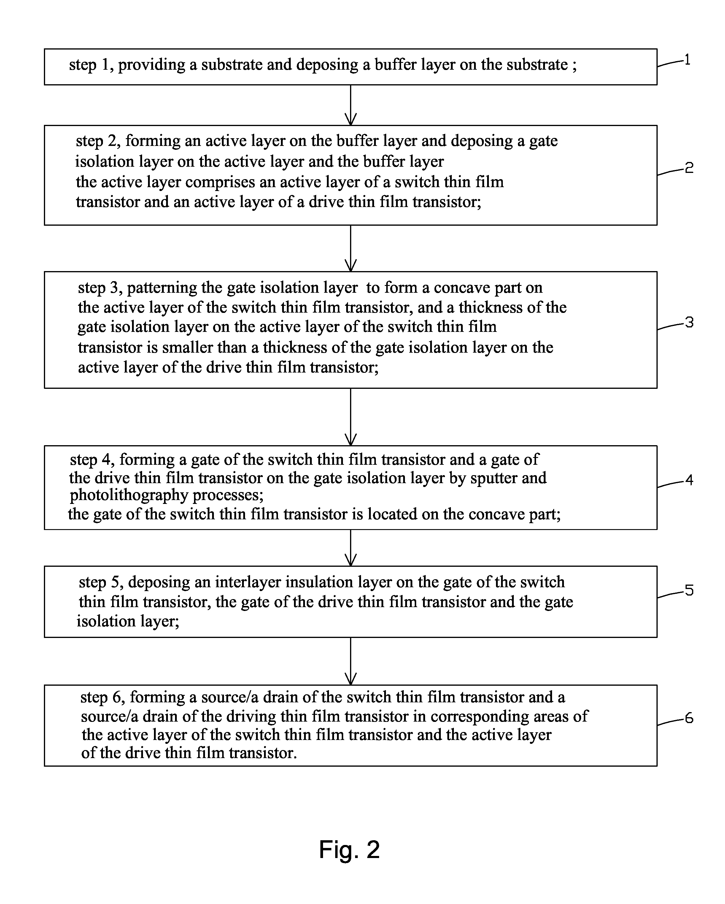
[0063]Please refer to FIG. 2. The present invention provides a manufacture method of a TFT backplate applicable to an AMOLED, comprising steps of:

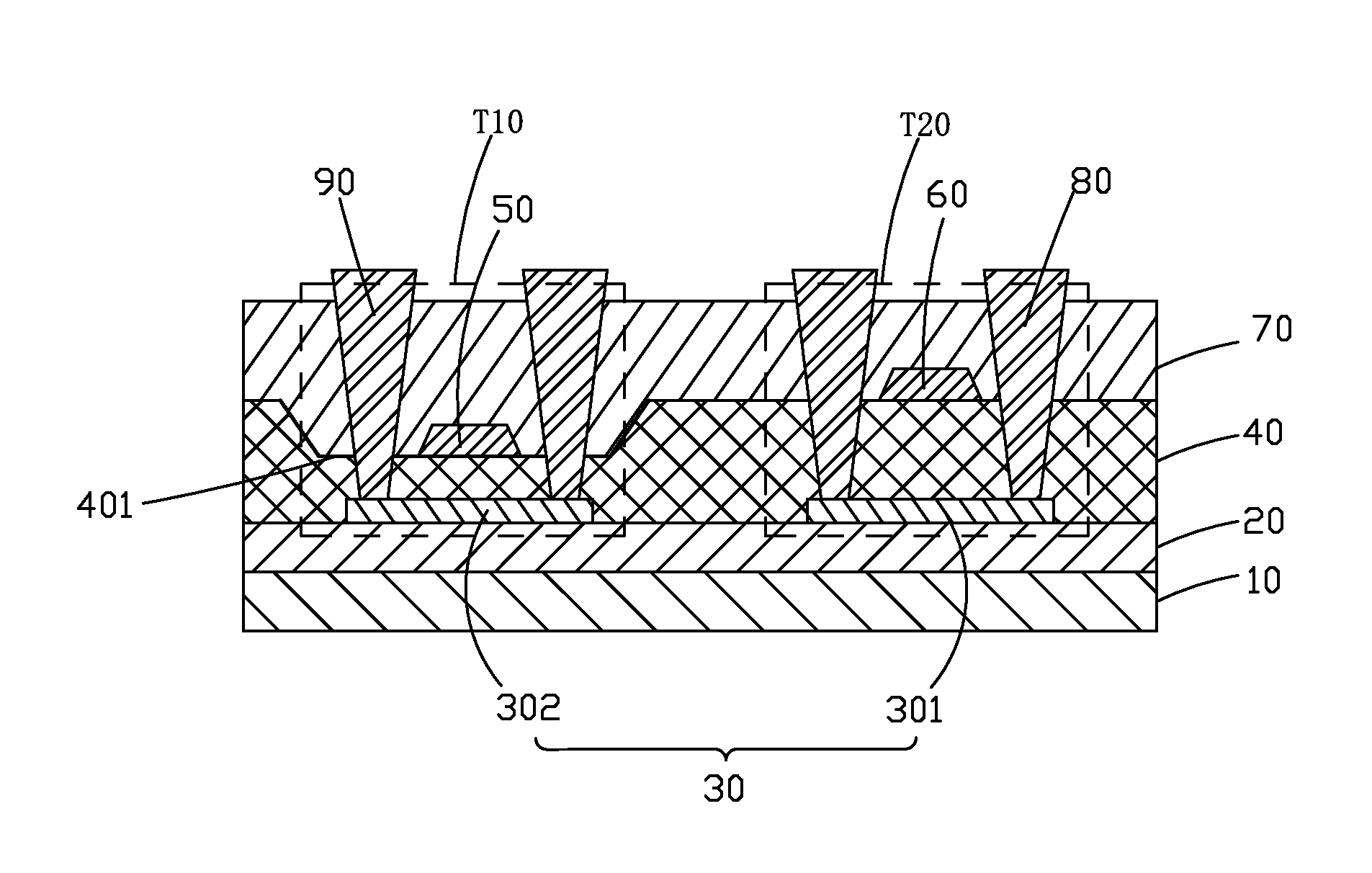
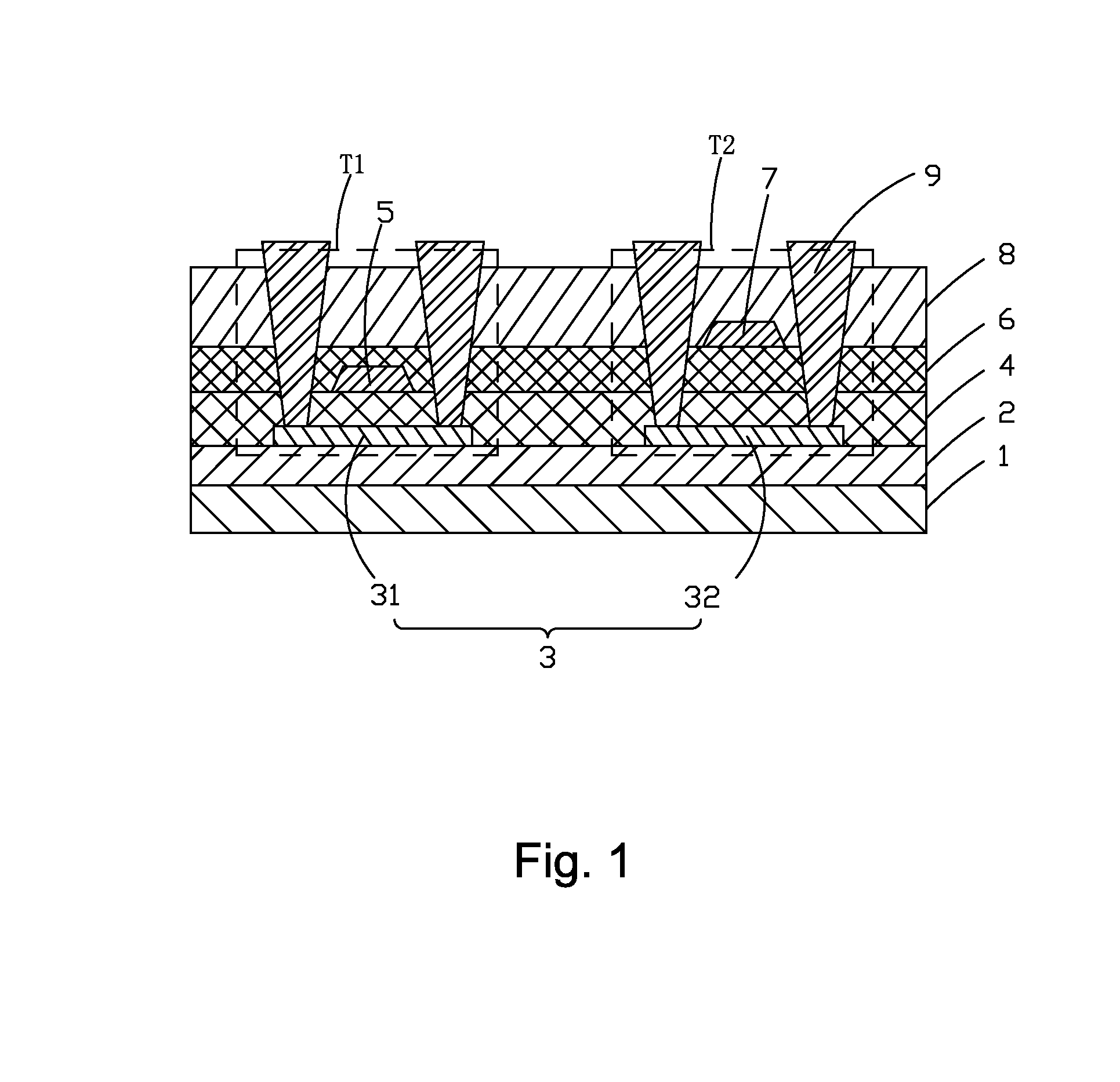
[0064]step 1, as shown in FIG. 3, providing a substrate 10 and deposing a buffer layer 20 on the substrate 10.

[0065]Specifically, the substrate 10 is a transparent substrate. Preferably, the substrate 10 is a glass substrate. The buffer layer 20 comprises one a silicon oxide layer, a silicon nitride or a combination thereof.

[0066]step 2, as shown in FIG. 4, forming an active layer 30 on the buffer layer 20 and deposing a gate isolation layer 40 on the active layer 30 and the buffer layer 20.

[0067]The active layer 30 comprises an active layer 302 of a switch thin film transistor and an active layer 301 of a drive thin film transistor....


PUM


Abstract

The present invention provides a manufacture method and a structure of a TFT backplate applicable to an AMOLED. The method comprises: step 1, providing a substrate (10) and deposing a buffer layer (20); step 2, sequentially forming an active layer (30) and a gate isolation layer (40) on the buffer layer (20); step 3, patterning the gate isolation layer (40) to form a concave part (401); step 4, forming a gate (50) of the switch thin film transistor and a gate (60) of the drive thin film transistor on the gate isolation layer, and the gate (50) of the switch thin film transistor is in the concave part (401); step 5, deposing an interlayer insulation layer (70). The method simplifies the manufacture process of the TFT backplate and increases the subthreshold swing of the drive thin film transistor by manufacturing a single layer gate isolation layer with height difference to raise the gray scale switch and control performance of the AMOLED panel.

Description

FIELD OF THE INVENTION[0001]The present invention relates to a display technology field, and more particularly to a manufacture method and a structure of a TFT backplate applicable to an AMOLED.BACKGROUND OF THE INVENTION[0002]The flat panel display elements possess many merits of thin frame, power saving, no radiation, etc. and have been widely used. The present flat panel display elements at present mainly comprise the Liquid Crystal Display (LCD) and the Organic Light Emitting Display (OLED).[0003]An OLED possesses many outstanding properties of self-illumination, no requirement of backlight, high contrast, ultra-thin, wide view angle, fast response, applicability of flexible panel, wide range of working temperature, simpler structure and process. The OLED is considered as next generation flat panel display technology.[0004]The OLED can be categorized as Passive matrix OLED (PMOLED) and (Active matrix OLED) AMOLED according to their driving types. The AMOLED possesses characters ...

Claims


Application Information

Patent Timeline
Patent Type & Authority Applications(United States)
IPC IPC(8): H01L27/12H01L21/265H01L29/786H01L21/28H01L21/285H01L21/02H01L29/66
CPCH01L27/1222H01L2227/323H01L21/02532H01L21/02592H01L21/02675H01L21/26506H01L29/66757H01L21/02271H01L21/02164H01L21/0217H01L27/1218H01L21/28079H01L27/1248H01L21/2855H01L21/28568H01L29/78675H01L27/3262H01L27/1274H01L27/1237H10K59/1213H10K50/00H10K59/1201
Inventor ZHANG, ZHANDONG
Owner TCL CHINA STAR OPTOELECTRONICS TECH CO LTD
Why Eureka
Try Eureka