Copper clad laminate for forming of embedded capacitor layer, multilayered printed wiring board, and manufacturing method of multilayered printed wiring board

a technology of embedded capacitors and copper clad laminates, which is applied in the formation of printed capacitors, other domestic articles, printed element electric connection formation, etc., can solve the problems of low voltage between the top electrode and the bottom electrode of the capacitor circuit, short circuit, etc., and achieve the effect of stable capacitan

Active Publication Date: 2016-11-10
MITSUI MINING & SMELTING CO LTD
View PDF2 Cites 5 Cited by
  • Summary
  • Abstract
  • Description
  • Claims
  • Application Information

AI Technical Summary

Benefits of technology

[0024]The copper clad laminate for forming of an embedded capacitor layer according to the present invention specifies the Young's modulus Er of a resin film constituting the dielectric layer of the capacitor along the thickness direction less than 6.1 GPa. The embedded capacitor layer in the multilayered printed wiring board embedded a capacitor circuit manufactured by using the copper clad laminate for forming of the embedded capacitor layer is prevented crack generation in drilling of the dielectric layer of the capacitor for boring of holes for forming of a through-hole. That is, as the multilayered printed wiring board embedded a capacitor circuit manufactured by using the copper clad laminate for forming of the embedded capacitor layer according to the present invention is provided with an excellent capacitor circuit without damage on the dielectric layer of the capacitor, the multilayered printed wiring board embedded a capacitor circuit achieves stable capacitance.
[0025]Generation of cracks in a dielectric layer in boring of holes for forming of a through-hole by drilling tend to be severe in a multilayered printed wiring board embedded a capacitor circuit having 8 or more layers. However, a multilayered printed wiring board embedded a capacitor circuit having 8 or more layers having holes for forming of a through-hole bored by drilling is provided a dielectric layer of the capacitor without generation of a crack if the manufacturing method of a multilayered printed wiring board embedded a capacitor circuit according to the present invention is employed.

Problems solved by technology

However, excessively thin dielectric layer has drawback that the break down voltage between the top electrode and the bottom electrode in the capacitor circuit becomes low and causes a short circuit.

Method used


Image

  • Copper clad laminate for forming of embedded capacitor layer, multilayered printed wiring board, and manufacturing method of multilayered printed wiring board
  • Copper clad laminate for forming of embedded capacitor layer, multilayered printed wiring board, and manufacturing method of multilayered printed wiring board
  • Copper clad laminate for forming of embedded capacitor layer, multilayered printed wiring board, and manufacturing method of multilayered printed wiring board

Examples


example 1

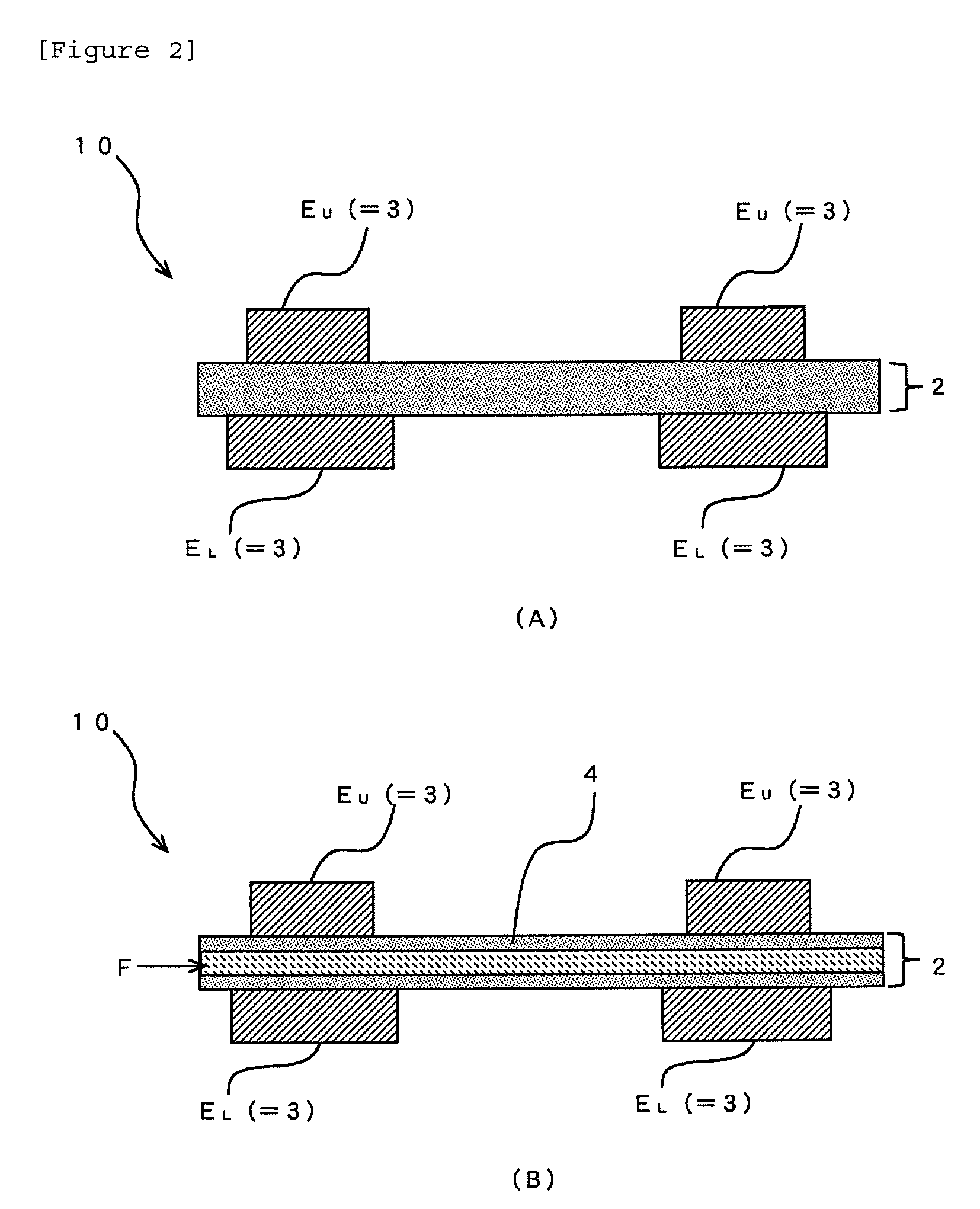
[0066]In Example 1, 26 layers multilayered printed wiring board embedded the capacitor circuit having the through-hole was manufactured through the following steps, and the presence or absence of crack generation in the dielectric layer of the capacitor 2 in the vicinity of the through-hole was investigated.

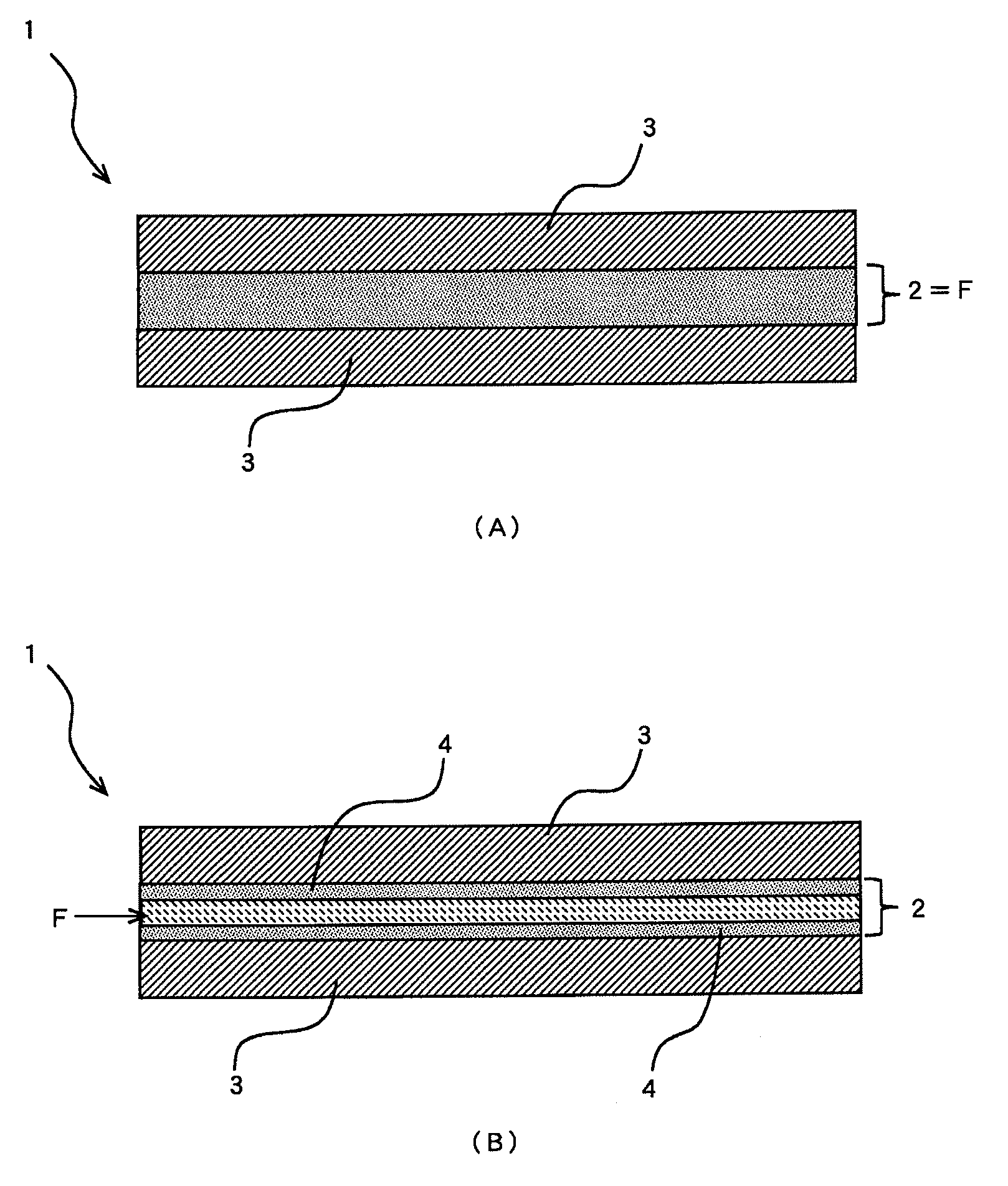
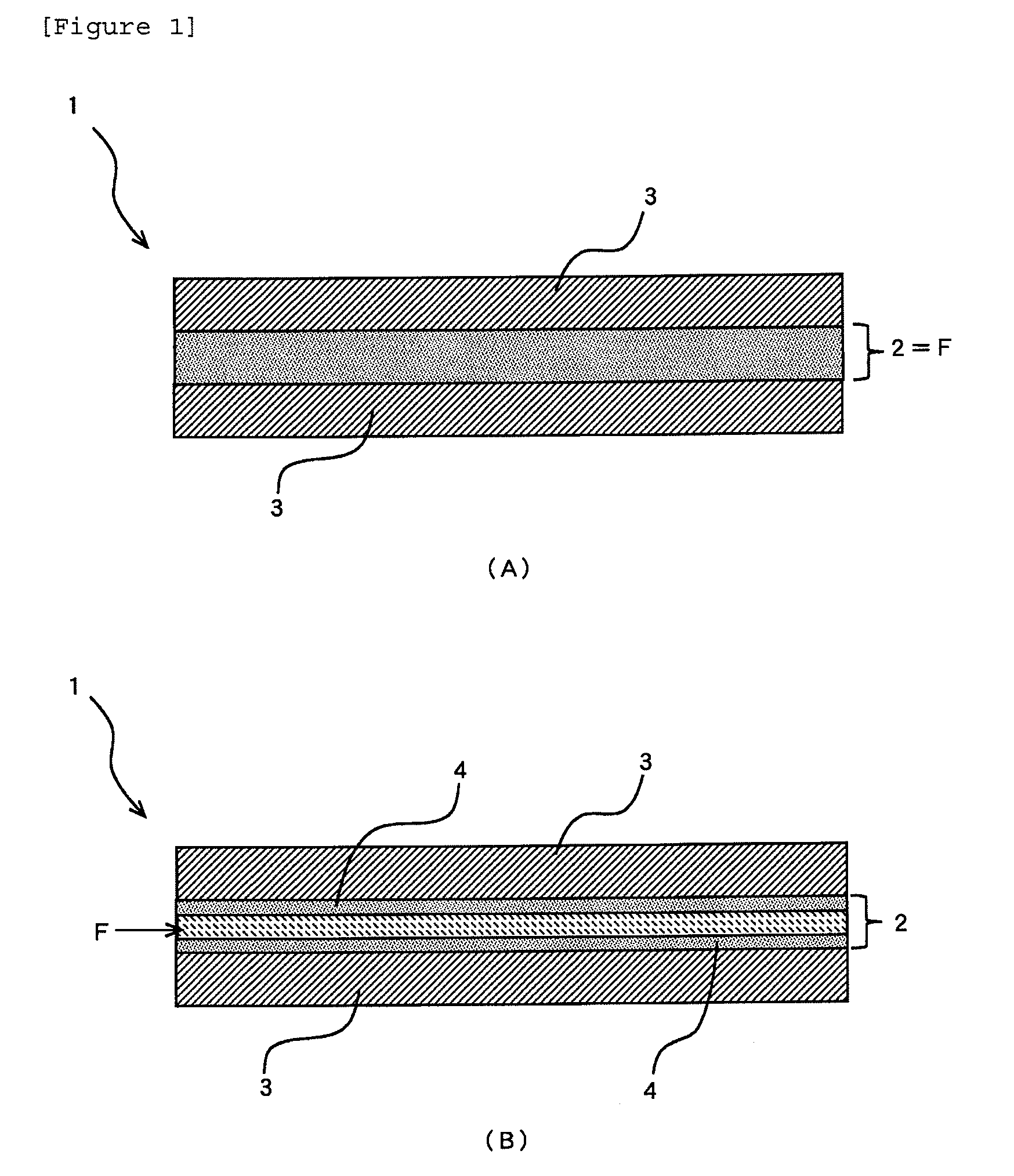
[0067]Manufacturing step of the copper clad laminate for forming of embedded capacitor layer: In the step, the copper clad laminate for forming of the embedded capacitor layer was manufactured by using the resin coated copper foil provided with the 5 μm thick semi-cured resin layer on the roughening treated surface of the 70 μm thick electrodeposited copper foil and the 12.5 μm thick polyimide resin film having the Young's modulus Er along the thickness direction of 5.87 GPa. The copper clad laminate for forming of the embedded capacitor layer 1 having the layer structure of “copper layer 3 / dielectric layer of the capacitor 2 (thickness: 22.5 μm) / copper layer 3” shown in FIG. 1 (...

example 2

[0075]In Example 2, the copper clad laminate for forming of the embedded capacitor layer 1 having the layer structure of “copper layer 3 / dielectric layer of the capacitor 2 (thickness: 24.2 μm) / copper layer 3” shown in FIG. 1 (B) was prepared in the same manner as in Example 1 except 14.2 μm thick polyimide resin film having the Young's modulus Er along the thickness direction of 2.66 GPa was used in place of the polyimide resin film used in Example 1, followed by preparing the 26 layers multilayered printed wiring board embedded a capacitor circuit having the through-hole. The presence or absence of the crack generation and the dimensional stability were investigated in the same manner as in Example 1. The results are shown in Table 1.


PUM

PropertyMeasurementUnit
Young's modulusaaaaaaaaaa
thicknessaaaaaaaaaa
thicknessaaaaaaaaaa

Abstract

Object is to provide a material for forming of the capacitor layer which generates no crack in drilling on the dielectric layer of the capacitor in manufacturing of a highly multilayered printed wiring board embedded a capacitor circuit. To achieve the object, copper clad laminate for forming of an embedded capacitor layer of a multilayered printed wiring board including an embedded capacitor circuit having a layer structure of copper layer / dielectric layer of the capacitor / copper layer in an inner layer characterized in that the Young's modulus Er of the resin film constituting the dielectric layer of the capacitor along the thickness direction is less than 6.1 GPa is employed.

Description

TECHNICAL FIELD[0001]The present invention relates to a copper clad laminate for forming of an embedded capacitor layer, a multilayered printed wiring board embedded a capacitor circuit, and a manufacturing method of the multilayered printed wiring board embedded a capacitor circuit.BACKGROUND ART[0002]In a multilayered printed wiring board in recent years, a multilayered printed wiring board embedded a capacitor circuit including a capacitor circuit in the inner layer has been employed as a power supply circuit / ground circuit to achieve a uniform power distribution and reduced noise generation. Also, high speed signal transmission in a device, stable power supply to the device for operation, power saving and reduction in noise generation are considered. In particular, such a multilayered printed wiring board embedded a capacitor circuit is one of a solution for mounting of LSI chips having increased wiring density and enlarged size used in a communication apparatus for infrastructu...

Claims


Application Information

Patent Timeline
Patent Type & Authority Applications(United States)
IPC IPC(8): H05K1/16H05K3/42H05K1/09B32B15/20H05K3/00H05K3/02H05K1/11B32B15/04H05K3/46H05K1/02
CPCH05K1/162H05K3/4623H05K3/429H05K1/09H05K1/0298H05K3/0047B32B2457/16H05K1/115B32B15/04B32B15/20H05K2201/09763B32B2457/00B32B2457/08H05K3/022B32B15/00B32B2307/51H05K3/4602H05K2201/0154H05K3/4644
Inventor KUWAKO, FUJIOMATSUSHIMA, TOSHIFUMIHOSOI, TOSHIHIRO
Owner MITSUI MINING & SMELTING CO LTD
Why Eureka
Try Eureka