Copper particle dispersing solution and method for producing conductive film using same

a technology of copper particle and solution, applied in the direction of conductive pattern formation, electrically conductive paints, transportation and packaging, etc., can solve the problems of complex process, inability to fire the paste, inability to form patterns on a substrate, etc., and achieve good storage stability and good electrical conductivity

Inactive Publication Date: 2016-12-01
DOWA ELECTRONICS MATERIALS CO LTD
View PDF9 Cites 41 Cited by
  • Summary
  • Abstract
  • Description
  • Claims
  • Application Information

AI Technical Summary

Benefits of technology

[0010]According to the present invention, it is possible to provide a copper particle dispersing solution, which has a good storage stability and which is able to form a conductive film having a good electrical conductivity with light firing, and a method for producing a conductive film using the same.

Problems solved by technology

), so that the process is complicated.
In addition, it is not possible to fire the paste with light irradiation, and it is not possible to form the pattern on a substrate, which is easily affected by heat, such as a paper or a polyethylene terephthalate (PET) film.
In the method disclosed in Japanese Patent Laid-Open No. 2010-528428, the storage stability of the copper ink solution containing copper nanoparticles (the copper particle dispersing solution) is not sufficient.
Moreover, if the conductive ink disclosed in Japanese Patent Laid-Open No. 2008-285761 is used as a copper particle dispersing solution for light firing, when the solution is applied on the substrate to be dried and fired with light irradiation to form the conductive film, cracks are formed in the conductive film to deteriorate the electrical conductivity of the film.

Method used


Image

  • Copper particle dispersing solution and method for producing conductive film using same

Examples


example 1

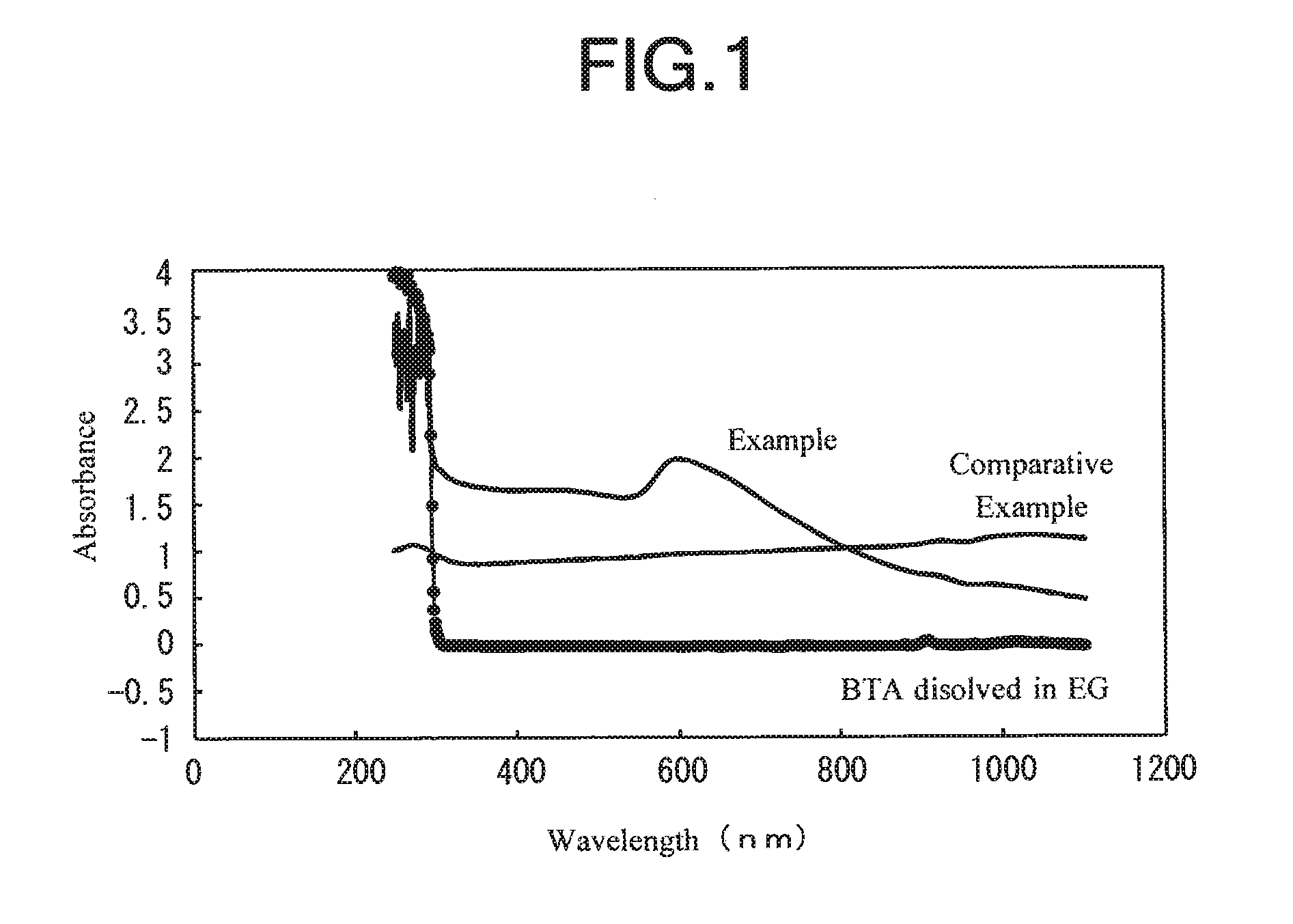
[0020]First, there were prepared 280 g of copper sulfate pentahydrate serving as a copper source, 1 g of benzotriazole (BTA) serving as a dispersing agent, a solution A obtained by dissolving 1 g of a water-based antifrothing agent (ANTIFLOTH F244 commercially available from DKS Co., Ltd.) in 1330 g of water, a solution B obtained by allowing 200 g of an aqueous solution containing 50% by weight of sodium hydroxide serving as a neutralizer to be diluted with 900 g of water, and a solution C obtained by allowing 150 g of an aqueous solution containing 80% by weight of hydrazine monohydrate as a reducing agent to be diluted with 1300 g of water.

[0021]Then, the solution A and the solution B were mixed with each other while being stirred, and the temperature of the mixed solution was adjusted to 60° C. Thereafter, while maintaining the stirring, all of the solution C was added to the mixed solution within 30 seconds. After about 5 minutes, the reaction was completed to produce a slurry....

example 2

[0034]A copper particle dispersing solution (conductive filler: 67% by weight) was obtained by the same method as that in Example 1, except that the ratio of the weight of the fine copper particles coated with BTA to the weight of the flake-shaped copper particles was 5:5.

[0035]This copper particle dispersing solution was used for producing a conductive film by flexographic printing by the same method as that in Example 1. Then, the electrical resistance (line resistance) of the conductive film was measured by the same method as that in Example 1, and the volume resistivity thereof was obtained by the same method as that in Example 1. As a result, when the thickness of the conductive film was μm, the electrical resistance (line resistance) thereof was 1.5Ω, and the volume resistivity thereof was 11 μΩ·cm. When the thickness of the conductive film was 4 μm, the electrical resistance (line resistance) thereof was 1.2Ω, and the volume resistivity thereof was 17 μΩ·cm. When the thicknes...

example [UNK]

Example 3˜5

[0037]Copper particle dispersing solutions (conductive filler: 67% by weight) were obtained by the same method as that in Example 1, except that spherical copper particles having an average particle diameter of 0.5 μm were used in place of the flake-shaped copper particles and that the ratio of the weight of the fine copper particles coated with BTA to the weight of the spherical copper particles was 1:9 (Example 3), 3:7 (Example 4) and 5:5 (Example 5), respectively.

[0038]These copper particle dispersing solutions were used for producing conductive films by flexographic printing by the same method as that in Example 1. Then, the electrical resistance (line resistance) of each of the conductive films was measured by the same method as that in Example 1, and the volume resistivity thereof was obtained by the same method as that in Example 1. As a result, with respect to the conductive film obtained by using the copper particle dispersing solution in Example 3, when the thic...


PUM

PropertyMeasurementUnit
particle diameteraaaaaaaaaa
pulse voltageaaaaaaaaaa

Abstract

A copper particle dispersing solution obtained by dispersing fine copper particles having an average particle diameter of 1 to 100 nm, each of the fine copper particles being coated with an azole compound, such as benzotriazole, and coarse copper particles having an average particle diameter of 0.3 to 20 μm in a dispersing medium, such as ethylene glycol, so as to cause the total amount of the fine copper particles and coarse copper particles to be 50 to 90% by weight and so as to cause the ratio of the weight of the fine copper particles to the weight of the coarse copper particles to be in the range of from 1:9 to 5:5, is applied on a substrate by screen printing or flexographic printing to be preliminary-fired with vacuum drying, and then, fired with light irradiation by irradiating light having a wavelength of 200 to 800 nm at a pulse period of 100 to 3000 μm and a pulse voltage of 1600 to 3600 V, to form a conductive film on the substrate.

Description

TECHNICAL FIELD[0001]The present invention relates generally to a copper particle dispersing solution. More specifically, the invention relates to a copper particle dispersing solution for use in the production of a conductive film for forming electrodes and circuits of electronic parts and so forth, and a method for producing a conductive film using the same.BACKGROUND ART[0002]As a conventional method for producing a conductive film using a copper particle dispersing solution, there is proposed a method for applying a photosensitive paste, which contains fine inorganic particles, such as fine glass particles, a photosensitive organic constituent, and a compound having an azole structure, such as benzotriazole, on a substrate to expose, develop and fire the paste to form a pattern (of a conductive film) (see, e.g., Japanese Patent Laid-Open No. 9-218508).[0003]There is also proposed a method for printing a copper ink solution containing copper nanoparticles (a copper particle dispe...

Claims


Application Information

Patent Timeline
Patent Type & Authority Applications(United States)
IPC IPC(8): B22F1/00B05D7/24H05K3/12B05D3/06B22F1/052B22F1/0545B22F1/102B22F1/16C09D7/62
CPCB22F1/0014B22F1/0022B05D3/06B05D7/24B22F2304/10H05K3/1208B22F2301/10B22F2304/054B22F2304/058H05K3/1216B22F9/24C09D5/24H01B1/22H05K1/097C08K9/04C08K2003/085C08K2201/005C09D7/62C09D7/67C09D7/68C09D7/69B22F1/0545B22F1/102B22F1/16B22F1/052C09D7/61
Inventor FUJITA, HIDEFUMIKANEDA, SHUJIITOH, DAISUKE
Owner DOWA ELECTRONICS MATERIALS CO LTD
Why Eureka
Try Eureka