
Top-emitting OLED substrate and fabrication method thereof, and display apparatus

a technology of top-emitting oled and substrate, which is applied in the direction of electrical equipment, basic electric elements, semiconductor devices, etc., can solve the problems of significant loss of light energy, relatively low external quantum efficiency of oled, and relatively low luminous efficiency, so as to improve the external quantum efficiency of the display substrate and reduce the loss of luminous efficiency

Active Publication Date: 2016-12-15
BOE TECH GRP CO LTD +1
View PDF3 Cites 1 Cited by
  • Summary
  • Abstract
  • Description
  • Claims
  • Application Information

AI Technical Summary

Benefits of technology

The present disclosure provides an organic light-emitting diode (OLED) substrate that can improve display efficiency and image quality. The substrate has a conductive layer with multiple anodes and cathodes, and a light-emitting layer electrically connecting the cathodes and anodes. By reducing the number of layers through which emitted light passes, the substrate reduces luminous efficiency loss caused by the light wave-guide effect and improves external quantum efficiency. Additionally, the substrate avoids the thickness limitation of cathodes and improves the reflective ability of the display substrate.

Problems solved by technology

The light energy can be significantly loss due to a light wave-guide effect during the light transport process.
Thus, there may be only a small amount of light emits from the OLED; and the luminous efficiency may be relatively low.
Therefore, the external quantum efficiency of the OLED may be relatively low.
If not, the external quantum efficiency of the top-emitting OLED may be substantially low; and the image quality and the display effect may be significantly impaired.
Therefore, how to improve the external quantum efficiency of OLED devices; and to reduce the luminous efficiency loss caused by the light wave-guide effect has become a demanding issue in the field of the display technologies.

Method used


Image

  • Top-emitting OLED substrate and fabrication method thereof, and display apparatus
  • Top-emitting OLED substrate and fabrication method thereof, and display apparatus
  • Top-emitting OLED substrate and fabrication method thereof, and display apparatus

Examples


Embodiment Construction

[0044]Reference will now be made in detail to exemplary embodiments of the invention, which are illustrated in the accompanying drawings. The detailed descriptions only illustrate certain exemplary embodiments of the present invention, and are not intended to limit the scope of the present invention.

[0045]According to the disclosed embodiments, a top-emitting organic light emitting diode (OLED) substrate is provided.

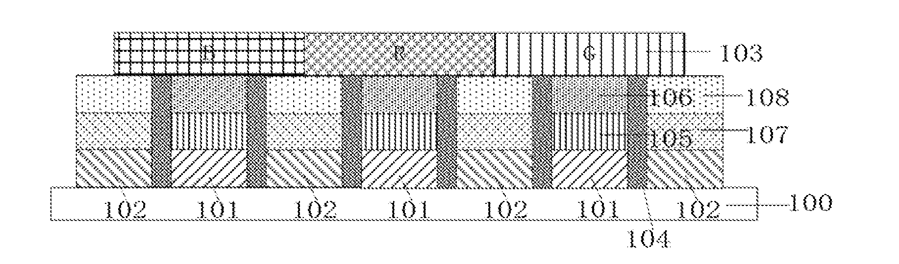
[0046]FIG. 2a illustrates an exemplary OLED substrate. As shown in FIG. 2a, the OLED substrate may include a substrate 100. Further, the OLED substrate may also include a plurality of anodes 101 and a plurality of cathodes 102 formed in a same layer over the substrate 100. The plurality of anodes 101 and the plurality of cathodes 102 may be electrically insulated. Further, the OLED substrate may also include a light-emitting layer 103. The light-emitting layer 103 may be electrically connected with the plurality of anodes 101 and the plurality of cathodes 102.

[0047]In or...


PUM


Abstract

An organic light-emitting diode substrate is provided. The organic light-emitting diode substrate comprises a substrate; a conductive layer formed over the substrate comprising a plurality of anodes and a plurality of cathodes, wherein each of the anodes are electrically insulated from the rest of the anodes and the cathodes; and a light-emitting layer formed over the plurality of anodes and the plurality of cathodes and being electrically connected with the plurality of anodes and the plurality of cathodes.

Description

CROSS-REFERENCES TO RELATED APPLICATIONS[0001]This PCT patent application claims priority of Chinese Patent Application No. 201510080227.6, filed on Feb. 13, 2015, the entire contents of which are incorporated by reference herein.FIELD OF THE INVENTION[0002]The present invention generally relates to the field of display technologies and, more particularly, to top-emitting OLED substrates and fabrication processes thereof, and a display apparatus.BACKGROUND[0003]Organic light emitting diode (OLED) display apparatus has many advantages, such as low power-consumption, high color saturation, wide viewing angle, ultra-thin structure, and flexible displaying ability, etc. Thus, it has become a mainstream technology in the display field.[0004]FIG. 1a illustrates a general structure of an OLED. As shown in FIG. 1a, the OLED includes a substrate 001, an anode 002, a light-emitting layer 003, and a cathode 004 sequentially formed on the substrate 001. When a voltage is applied between the ano...

Claims


Application Information

Patent Timeline
IPC IPC(8): H01L27/32H01L51/52H01L51/56
CPCH01L27/3206H01L51/56H01L51/5259H01L51/5221H01L51/5253H01L51/5218H10K59/35H10K2102/3026H10K59/805H10K59/873H10K59/30H10K50/82H10K50/805H10K50/818H10K50/844H10K50/846H10K71/00
Inventor YANG, WENBINCHANG, QINGHUANG, JINHAOWANG, XIANGNAN
Owner BOE TECH GRP CO LTD
Learn More