Wavelength emitting electronic device

a wavelength emitting electronic and wavelength-emitting technology, applied in the field of light emitting apparatuses, can solve the problems of complex light-sensing systems, high power requirements and cost incurred by conventional light sources, and achieve the effects of enhancing growth, enhancing growth, and reducing power consumption requirements

Active Publication Date: 2016-12-22
MARTIN ELIZABETH A
View PDF1 Cites 2 Cited by
  • Summary
  • Abstract
  • Description
  • Claims
  • Application Information

AI Technical Summary

Benefits of technology

[0006]The invention disclosed herein addresses the abovementioned need for a light emitting apparatus, which provides the necessary power spectral density (PSD) of Photosynthetic Active Radiation (PAR) with minimal power consumption requirements. Furthermore, the invention addresses the need for a light emitting apparatus, which is capable of selectively supplying wavelengths of light that enhance growth and allow for controlled manipulation of all higher forms of plant life. The wavelength emitting electronic device, designed for enhancing growth of a plurality of plants disclosed herein, includes a supporting frame member, at least one printed circuit board, and an optically transmittive material. The supporting frame member includes a first surface and a second surface. The printed circuit board includes an array of light sources. In an embodiment, the printed circuit board is detachably attached to the second surface of the supporting frame. The array of light sources receives electrical signals from a class 2 circuit rectification module power source. Each light source of the array of light sources only emits light of predetermined wavelengths. The optically transmittive material is fixedly attached to the supporting frame member for transmitting light emitted by the array of light sources to plants for enhancing growth and controlled manipulation.

Problems solved by technology

However, the abovementioned light sources are energy intensive, which means the power outputs of some of these lamps range from about 400 W to 1100 W. In commercial indoor horticultural applications, several of these lamps may be required to direct light over a large area.
The power requirements and the costs incurred for conventional light sources are thus high.
Furthermore, photoreceptors, which are complex light-sensing systems within plants, respond to energy packets carried at specific wavelength signals measured in nanometers.

Method used


Image

  • Wavelength emitting electronic device
  • Wavelength emitting electronic device
  • Wavelength emitting electronic device

Examples


Embodiment Construction

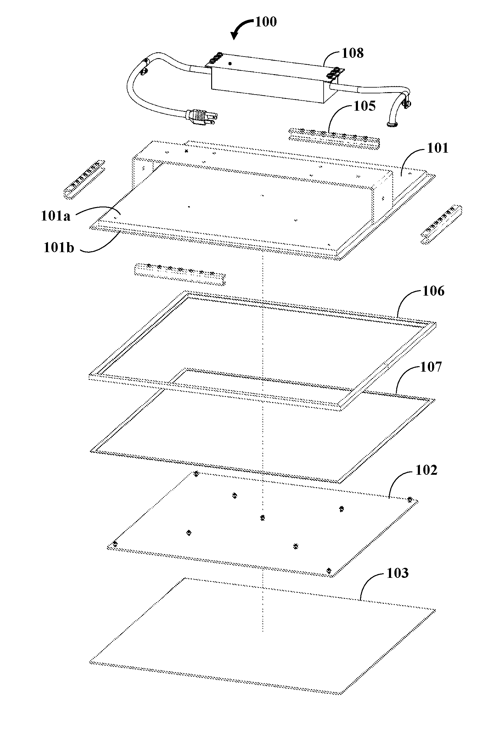
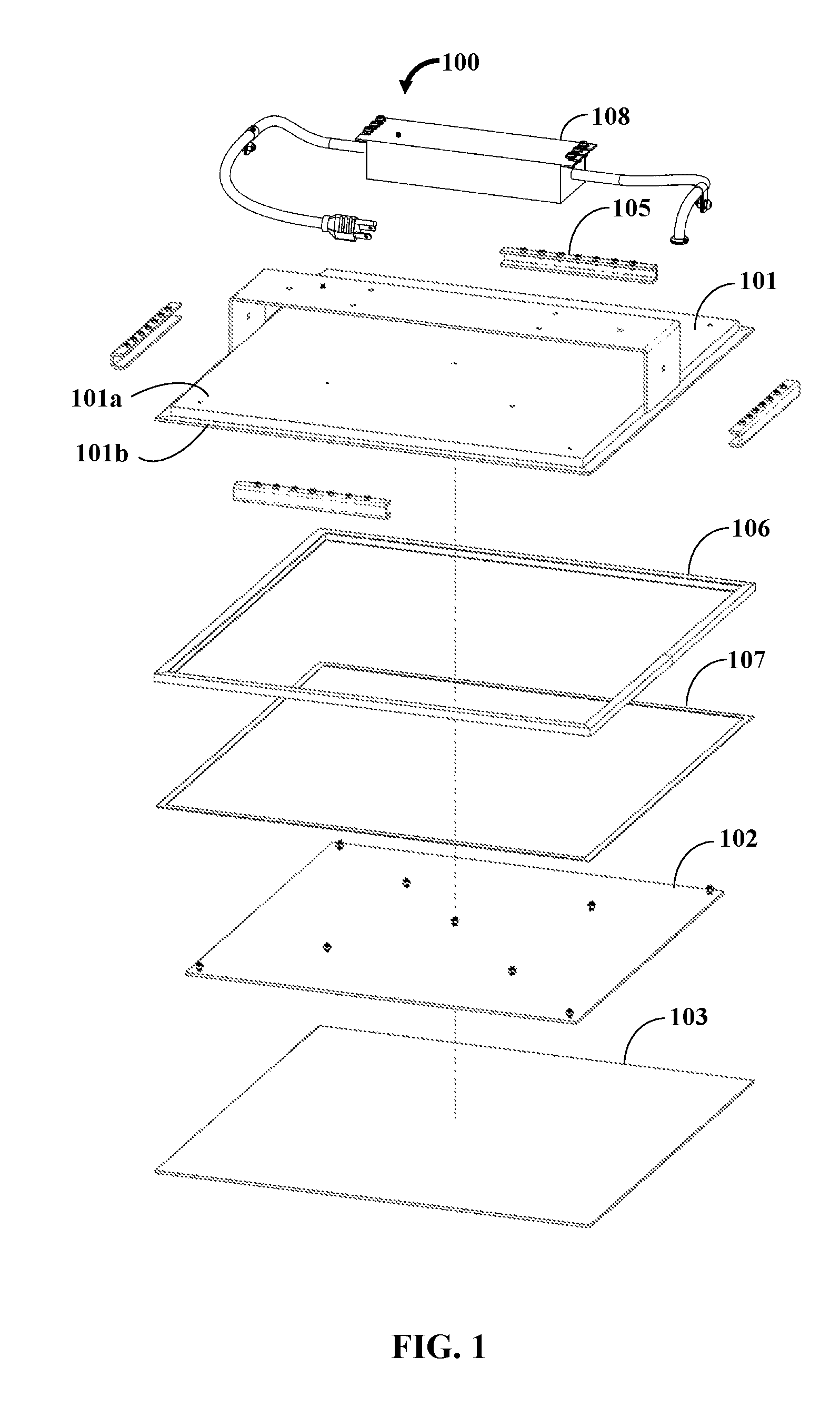
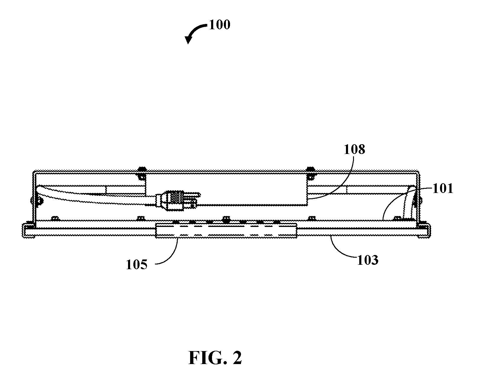
[0017]FIG. 1 exemplarily illustrates an exploded view of a wavelength emitting electronic device 100. The wavelength emitting electronic device 100 is an optoelectronic device that creates photonic effects. As used herein, “optoelectronic devices” refer to devices or circuits that comprise both electrical and optical functions, i.e., a thin-film semiconductor device. Optoelectronic devices function as electrical-to-optical transducers or optical-to-electrical transducers. As used herein, “photonics” refers to the particle properties of light, wavelength identification, the potential of creating signal processing device technologies using photons distribution and / or manipulation, the practical application of optics and uses in the marketplace, and an analogy to electronics. The wavelength emitting electronic device 100 disclosed herein, employs both, former and the latter. Optoelectronics is based on the quantum mechanical effects of light on electronic materials, especially semicond...


PUM


Abstract

A wavelength emitting electronic device for enhancing growth of a plurality of plants includes a supporting frame member, at least one printed circuit board (PCB), and an optically transmittive material. The supporting frame member includes a first surface and a second surface. The PCB includes an array of light sources. The PCB is detachably attached to the second surface of the supporting frame. The array of light sources receives electrical signals from a circuit rectification module power source. Each light source of the array of light sources emits light of predetermined wavelengths. The optically transmittive material is fixedly attached to the supporting frame member for transmitting the light emitted by the array of light sources to the plants for enhancing growth of plants.

Description

FIELD OF THE INVENTION[0001]The present invention disclosed herein specifically relates to light emitting apparatuses for enhancing growth of plant life through use of wavelength manipulation. This invention herein to be referred to as a wavelength emitting electronic device. More particularly, the invention disclosed herein relates to a wavelength emitting electronic device for manipulating plant growth using restricted spectral output wavelengths to target chemical excitation with chlorophyll molecules in chloroplast.BACKGROUND[0002]The effects of light on the growth of plants have been studied over the years. Several studies have shown that by manipulating the wavelengths and duration of light directed at a selection of plant, their growth can be enhanced or reduced. Tissue culture, used widely in plant science, is the growth of plant tissues or cells within a controlled environment. Traditionally, tissue culture researchers' and horticultural industries have used artificial ligh...

Claims


Application Information

Patent Timeline
Patent Type & Authority Applications(United States)
IPC IPC(8): A01G7/04F21V3/04F21V23/02F21V21/00F21V17/10
CPCA01G7/045F21V21/00F21V17/10F21Y2115/15F21V3/0418F21Y2115/10F21V23/02F21V3/061Y02P60/14
Inventor MARTIN, ELIZABETH A
Owner MARTIN ELIZABETH A
Why Eureka
Try Eureka