Epitaxial growth of gallium arsenide on silicon using a graphene buffer layer

a technology of graphene buffer layer and gallium arsenide, which is applied in the direction of basic electric elements, electrical equipment, semiconductor devices, etc., can solve the problems of thermal expansion mismatch, lattice mismatch, thermal expansion mismatch, and dissimilar chemical bonding, and achieve the heteroepitaxial growth of gaas/si. the effect of increasing the number of peaks

Inactive Publication Date: 2017-02-16
KING ABDULAZIZ CITY FOR SCIENCE AND TECHNOLOGY +1
View PDF4 Cites 17 Cited by
  • Summary
  • Abstract
  • Description
  • Claims
  • Application Information

AI Technical Summary

Benefits of technology

[0014]Accordingly, a need exists for advanced techniques for employing van der Waals growth of GaAs on silic

Problems solved by technology

While nearly perfect homoepitaxial growth was demonstrated by MBE, heteroepitaxial growth is challenged by dissimilar chemical bonding, surface dangling bonds, surface states, and surface symmetry mismatch.
In addition, lattice mismatch, polar-on-non-polar epitaxy, and thermal expansion mismatch add complexity to the direct heteroepitaxial growth of GaAs/Si.
Nevertheless, successful operation of NW-based devices is impeded by carrier loss mechanisms, surf

Method used


Image

  • Epitaxial growth of gallium arsenide on silicon using a graphene buffer layer
  • Epitaxial growth of gallium arsenide on silicon using a graphene buffer layer
  • Epitaxial growth of gallium arsenide on silicon using a graphene buffer layer

Examples


Embodiment Construction

1. Introduction

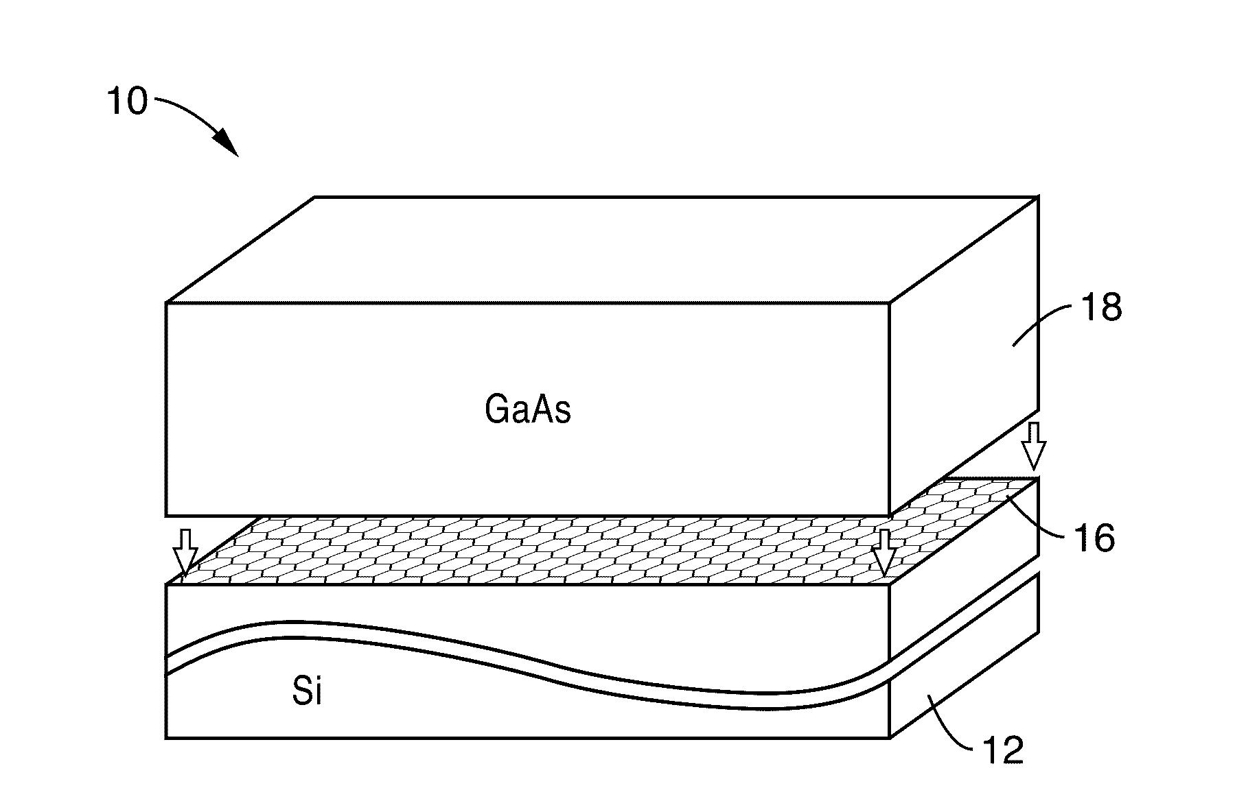
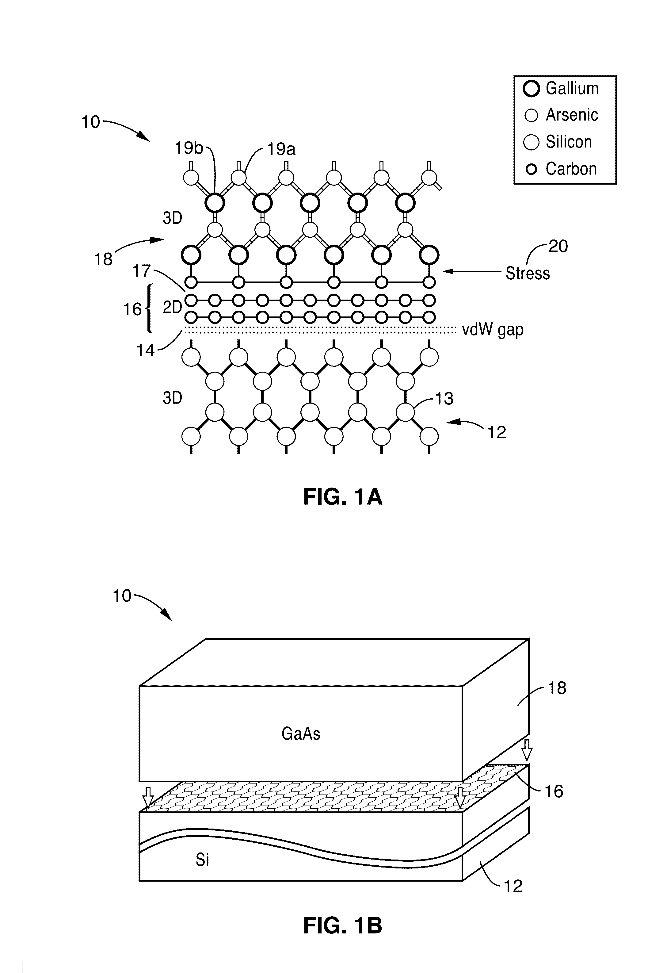
[0027]Van der Waals epitaxy (vdWE) has been proven to be a useful route to heteroepitaxy. Utilizing vdWE, depositing a material with three-dimensional (3D) bonding on a two-dimensional (2D) layered van-der-Waals material could be a new and interesting approach of heteroepitaxy. The bonds between the 2D material / upper 3D epilayer in this approach are about two orders of magnitude weaker in comparison to the covalent bonds between the 3D substrate / 3D deposited layer. Therefore, the weak bonds between 2D / 3D could accommodate thermal mismatch with different substrate temperatures during the growth. Furthermore, the strain due to the in-plane lattice-mismatch with the epitaxially-grown 3D overlayers is mitigated in quasi-van der Waals Epitaxy (QvdWE) due to low growth-axis bond energies. Considering further, the dislocations at the interface are not expected to propagate through the grown material due to the weak interactions at 2D / 3D heterointerface. Only the topmost laye...


PUM


Abstract

Epitaxial growth of gallium arsenide (GaAs) on a semiconductor material (e.g., Si) using quasi-van der Waals Epitaxy (QvdWE). Prior to GaAs growth a buffer layer (e.g., graphene) is deposited which relieves lattice mismatch/thermal expansion. The low energy of the graphene surface and the GaAs/graphene interface is overcome through an optimized growth technique to obtain an atomically smooth low-temperature GaAs nucleation layer. The disclosure can be applied to optimize epitaxial thin film growth of other materials, (e.g., III-V semiconductors, such as InP, GaSb) on Si using van der Waals buffer layers such as graphene.

Description

CROSS-REFERENCE TO RELATED APPLICATIONS[0001]This application claims priority to, and the benefit of, U.S. provisional patent application Ser. No. 62 / 204,513 filed on Aug. 13, 2015, incorporated herein by reference in its entirety.STATEMENT REGARDING FEDERALLY SPONSORED RESEARCH OR DEVELOPMENT[0002]Not ApplicableINCORPORATION-BY-REFERENCE OF COMPUTER PROGRAM APPENDIX[0003]Not ApplicableNOTICE OF MATERIAL SUBJECT TO COPYRIGHT PROTECTION[0004]A portion of the material in this patent document is subject to copyright protection under the copyright laws of the United States and of other countries. The owner of the copyright rights has no objection to the facsimile reproduction by anyone of the patent document or the patent disclosure, as it appears in the United States Patent and Trademark Office publicly available file or records, but otherwise reserves all copyright rights whatsoever. The copyright owner does not hereby waive any of its rights to have this patent document maintained in...

Claims


Application Information

Patent Timeline
IPC IPC(8): H01L21/02H01L29/04H01L29/20
CPCH01L21/02485H01L29/045H01L21/02422H01L21/02389H01L21/0242H01L21/02444H01L21/02488H01L21/02546H01L21/02543H01L21/02549H01L21/0254H01L21/02609H01L21/02057H01L29/20H01L21/02381H01L21/02458H01L21/0262H01L21/02631
Inventor WANG, KANG L.ALASKAR, YAZEED
Owner KING ABDULAZIZ CITY FOR SCIENCE AND TECHNOLOGY
Why Eureka
Try Eureka