
Method for forming sin or sicn film in trenches by peald

a technology trenches, which is applied in the direction of chemical vapor deposition coating, coating, metal material coating process, etc., can solve the problems of poor sidewall or bottom surface coverage of sin or sicn film deposited in trenches of substrates, poor step coverage, and poor sidewall and bottom surface coverage of precursors

Inactive Publication Date: 2017-02-23
ASM IP HLDG BV
View PDF14 Cites 277 Cited by
  • Summary
  • Abstract
  • Description
  • Claims
  • Application Information

AI Technical Summary

Benefits of technology

The patent describes a new type of compound that can be used to form films in semiconductor devices. This compound has a unique bond structure that allows for better coverage of the film in the trenches and holes of the device. By using this new compound, the film quality on the sides and bottom of the device can be improved. This is achieved by incorporating a halogen group in the compound, which makes it easier to form a Si-N bond in the film and also allows for nitridization, resulting in a better film quality.

Problems solved by technology

When a SiN or SiCN film is formed by PEALD using a precursor having a nitrogen atom in the center of its skeletal structure where a terminal group of Si is terminated with a hydrogen or hydrocarbon, a sidewall or bottom surface coverage of the film deposited in a trench of a substrate is often insufficient due to its weak chemisorption properties.
However, the precursor still has a problem of poor sidewall and bottom surface coverage.
Conventionally, reaction groups and terminal groups of a precursor are constituted by mostly alkylamine or hydrogen, resulting in poor step coverage.
If nitridization depends predominantly on a plasma as in conventional precursors, not only step coverage but also film quality will often suffer, e.g., film quality on a blanket surface (a top surface in which a trench is formed) and a bottom surface will often be different, and film quality on a sidewall will often be unsatisfactory.

Method used


Image

  • Method for forming sin or sicn film in trenches by peald
  • Method for forming sin or sicn film in trenches by peald
  • Method for forming sin or sicn film in trenches by peald

Examples


examples

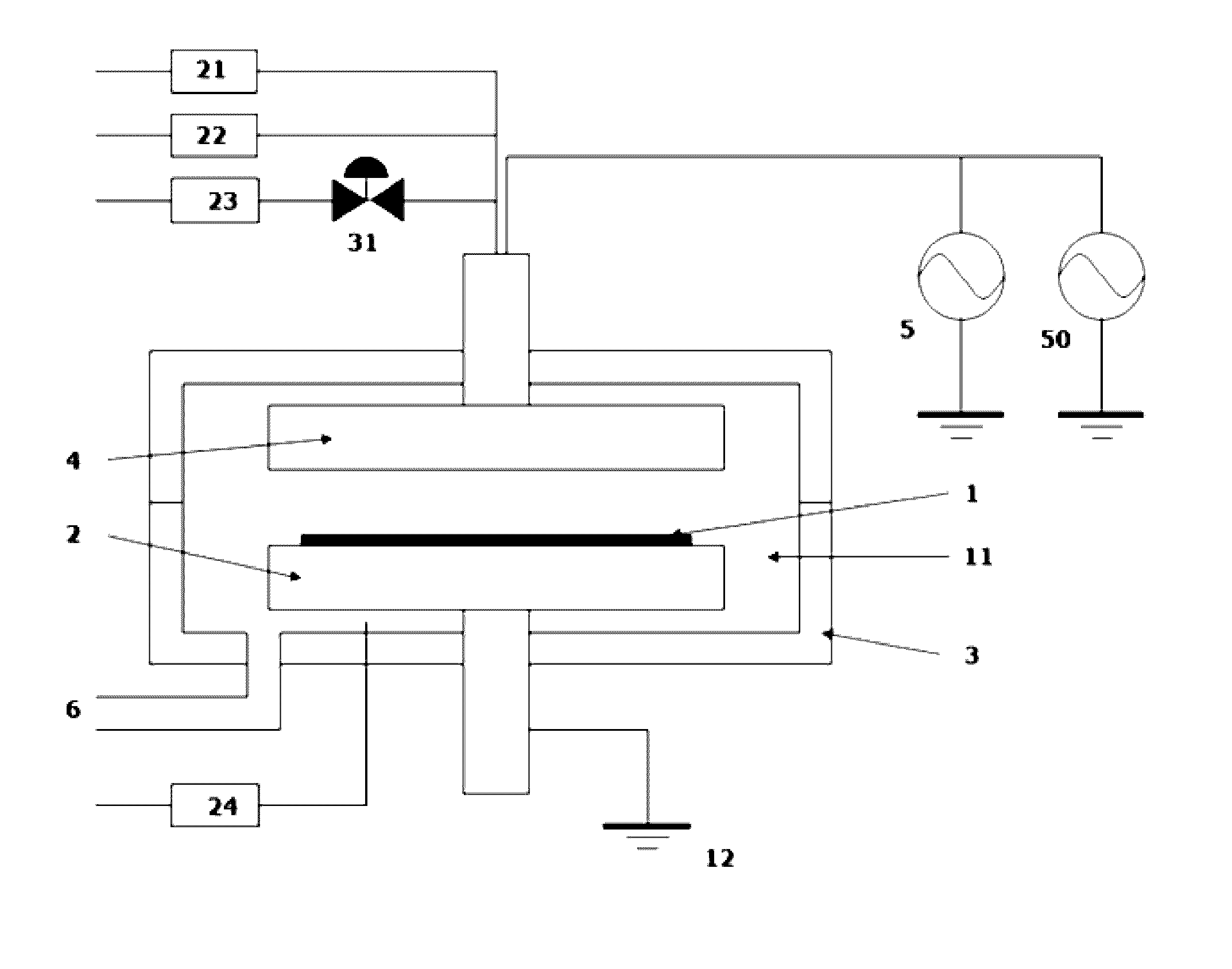
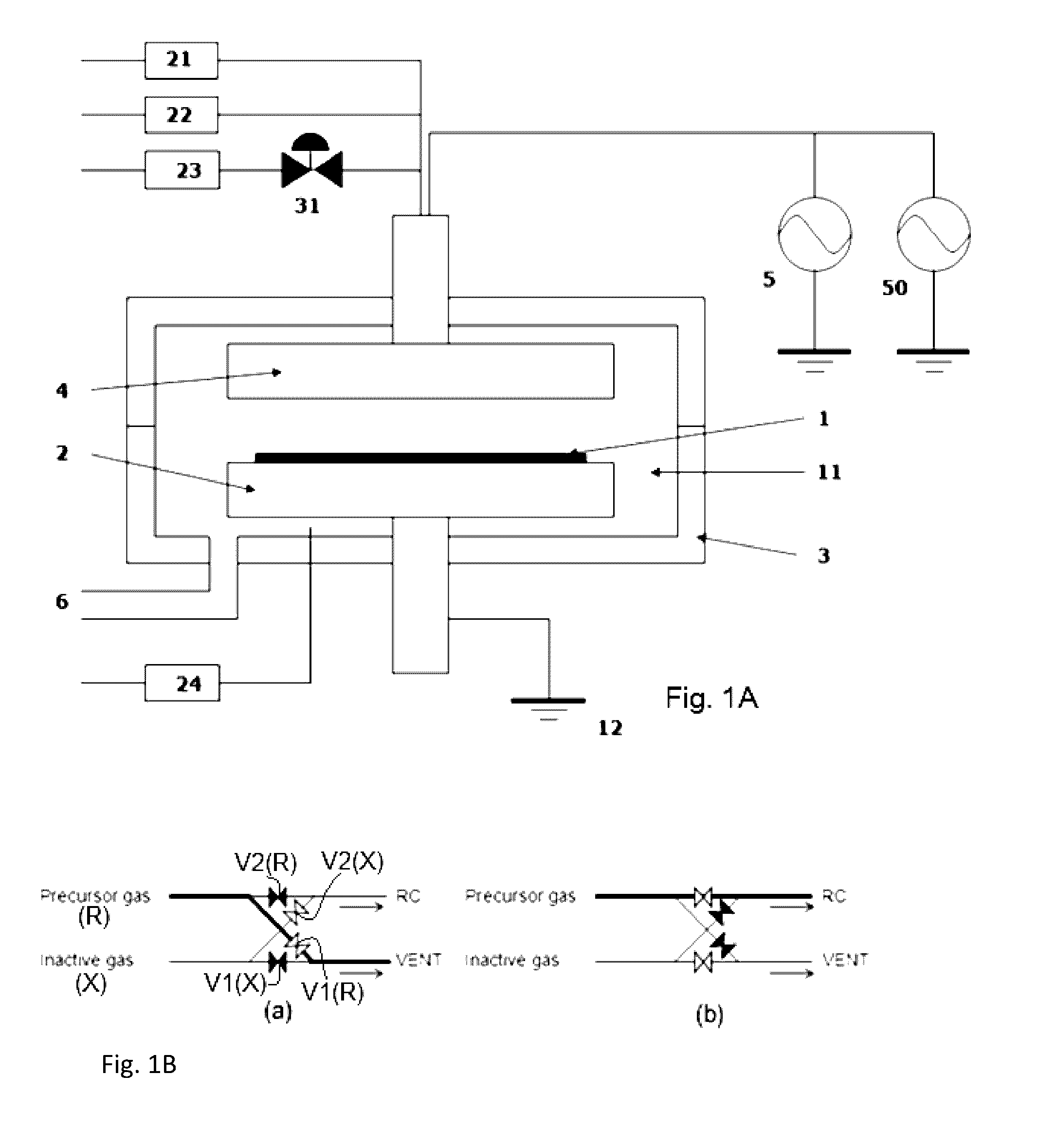
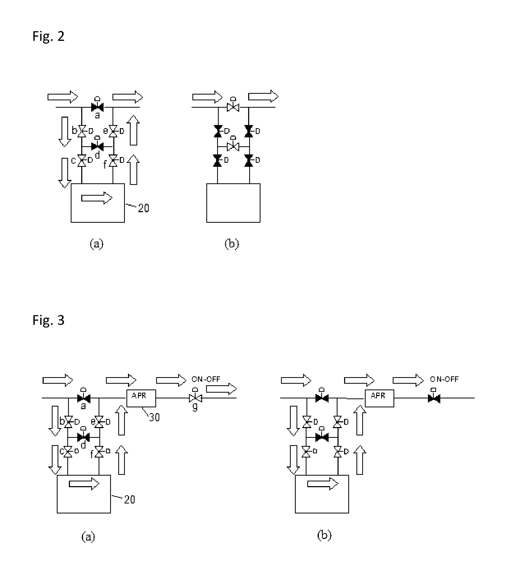
[0052]A SiN or SiCN film was formed on a Si substrate (Φ300 mm) having trenches with an aspect ratio of 3 (a width of 35 nm) by PEALD using a sequence illustrated in FIG. 7, one cycle of which was conducted under the common conditions shown in Table 3 (deposition cycle) below using the PEALD apparatus illustrated in FIG. 1A and a gas supply system (FPS) illustrated in FIG. 2 with the specific conditions and sequence indicated in Table 4.

TABLE 3(the numbers are approximate)Common Conditions for Deposition CycleSubstrate temperature350° C.Pressure400 PaCarrier gasArDilution gasArFlow rate of carrier gas (continuous)2000 sccmFlow rate of dilution gas (continuous)500 sccmRF power pulse5 secPurge after RF power pulse1 sec

TABLE 4(the numbers are approximate)ReactantRFFeed pulse / Precursor(flow rate)[W]Purge [sec]*1TrisilylamineNH3 (2 slm)1000.1 / 1*2TrisilylamineH2 / N2 (1 / 1 slm)1000.1 / 13TrischlorotrisilylamineNH3 (2 slm)1000.5 / 14TrischlorotrisilylamineH2 / N2 (1 / 1 slm)1000.5 / 15Monochlorotrisily...


PUM

PropertyMeasurementUnit
Fractionaaaaaaaaaa
Thicknessaaaaaaaaaa

Abstract

A method for forming a SiN or SiCN film in a trench on a substrate by plasma-enhanced atomic layer deposition (PEALD) conducts one or more process cycles, each process cycle including: (i) feeding a precursor in a pulse to a reaction space where the substrate is place, said precursor having a Si—N—Si bond in its skeletal structure to which at least one halogen group is attached; and (ii) applying RF power to the reaction space in the presence of a reactant gas and in the absence of any precursor to form a monolayer constituting a SiN or SiCN film.

Description

BACKGROUND[0001]Field of the Invention[0002]The present invention relates generally to a method forming a SiN or SiCN film in trenches on a substrate by plasma-enhanced atomic layer deposition (PEALD).[0003]Related Art[0004]When a SiN or SiCN film is formed by PEALD using a precursor having a nitrogen atom in the center of its skeletal structure where a terminal group of Si is terminated with a hydrogen or hydrocarbon, a sidewall or bottom surface coverage of the film deposited in a trench of a substrate is often insufficient due to its weak chemisorption properties. This may be because the precursor has only a Si—H bond as a chemisorption site. Among precursors having a nitrogen atom in the center of its skeletal structure, a compound having a silylamine structure is beneficial because the precursor has a Si—N—Si bond, and the skeleton of the deposited film can be derived from the precursor itself, and thus, the deposition of the film need not be dependent upon reaction with a reac...

Claims


Application Information

Patent Timeline
IPC IPC(8): C23C16/455C23C16/44C23C16/505C23C16/34
CPCC23C16/45536C23C16/345C23C16/347C23C16/4408C23C16/45553C23C16/505C23C16/045C23C16/36C23C16/5096
Inventor FUKAZAWA, ATSUKIFUKUDA, HIDEAKI
Owner ASM IP HLDG BV
Learn More