Method of manufacturing rim type of photomask and photomask made by such method

a technology of photomasks and rims, which is applied in the field of manufacturing rim types of photomasks, can solve the problems of large diffraction angle of exposure light passing through the mask, insufficient contrast of image being transferred by diffracted light, and expensive equipment such as electron beams and/or laser equipment, etc., and achieves a relatively simple method and uniform width

Inactive Publication Date: 2009-12-15
SAMSUNG ELECTRONICS CO LTD
View PDF7 Cites 0 Cited by
  • Summary
  • Abstract
  • Description
  • Claims
  • Application Information

AI Technical Summary

Benefits of technology

[0017]Another object of the present invention is to provide a relatively simple method of manufacturing a rim mask, and that does not require the need for relatively expensive processing equipment.
[0024]According to the present invention, a film having poor step coverage is formed on a quartz substrate having a 180°-phase shift region, and a 0°-phase shift region covered by a patterned light blocking (e.g., chrome) layer. Accordingly, the outer peripheral portion of the patterned light blocking layer can be exposed without subjecting the film to a lithography process such as an electron beam lithography process. The exposed portion of the patterned light blocking layer is then selectively removed using the film as an etch mask to form a light blocking pattern on the 0°-phase shift region and to expose the substrate at the border of the 0°-phase shift region. That is, the rim of the photomask can be formed without charging the film, from which the etch mask is formed, with electrons and developing the film. Thus, the method is relatively simple. Also, the light blocking pattern will have the desired shape, i.e., one that delimits the border of the 0°-phase shift region such that the border has a uniform width.

Problems solved by technology

However, if a line width of the opaque pattern is smaller than the wavelength (λ) of the exposure light, the angle of diffraction of the exposure light passing through the mask is too great for the exposure light to be focused on the pupil lens of the exposure apparatus, and the image being transferred by the diffracted light will not have a sufficient amount of contrast.
Therefore, it is problematic to use a binary mask having an opaque pattern to form a fine circuit pattern, i.e., a circuit pattern having a small line width.
However, the following problems arise when manufacturing the rim mask.
In addition, expensive equipment such as electron beam and / or laser equipment is required for rectifying any misalignment which may occur between the second photoresist pattern 16 and the etched chrome layer 12.
However, such a laser provides inferior exposure in a region that has a dimension on the order of microns, such as the region corresponding to the border 10c. A process of employing a conductive polymer in order to discharge the electrons has also been suggested, but is expensive and complicated.

Method used


Image

  • Method of manufacturing rim type of photomask and photomask made by such method
  • Method of manufacturing rim type of photomask and photomask made by such method
  • Method of manufacturing rim type of photomask and photomask made by such method

Examples


Embodiment Construction

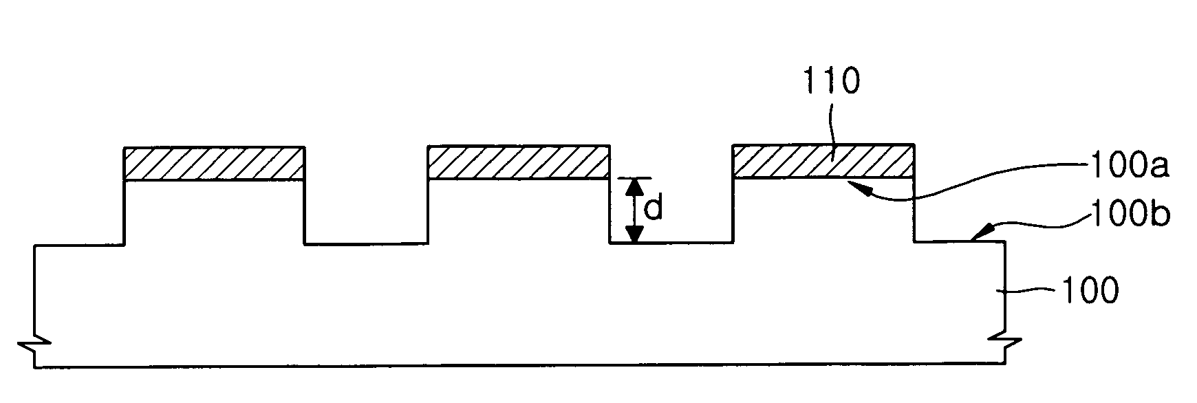
[0033]Hereinafter, a first embodiment of a method of manufacturing a rim mask according to the present invention will be described in detail with reference to FIGS. 4A through 4C.

[0034]Referring first to FIG. 4A, a chrome layer is formed on top of a quartz substrate 100 and a photoresist pattern (not illustrated) is formed on the chrome layer using electron beam lithography. The photoresist pattern exposes a portion of the chrome layer where the 180° phase shift region 100b of the rim mask is to be formed. The chrome layer is anisotropically etched using the photoresist pattern as a mask to thereby form a patterned chrome layer 110. The quartz substrate 100 is etched to a predetermined depth d using the patterned chrome layer 110 and the photoresist pattern as a mask to define the 180°-phase shift region 100b. The region of the quartz substrate 100 left covered by the patterned chrome layer 110 is a 0°-phase shift region 100a. The depth d of the 180°-phase region 100b is selected to...


PUM

PropertyMeasurementUnit
refractive indexaaaaaaaaaa
widthaaaaaaaaaa
widthaaaaaaaaaa

Abstract

A method of forming a rim type of photomask prevents a chrome pattern formed in the 0°-phase shift region of the mask substrate from being irregular and hence, ensures that the border of the 0°-phase shift region has a uniform width. First, a light blocking layer is formed on a quartz substrate. A select portion of the light blocking layer is etched to form a patterned light blocking layer, and the underlying quartz substrate is etched to a predetermined depth to form a 180°-phase shift region. Then, a fluid material layer is formed on the quartz substrate without an electron beam lithography process. The fluid material layer covers a central portion of the patterned light blocking layer and leaves an outer peripheral portion of the patterned light blocking layer exposed. Subsequently, the patterned light blocking layer is etched using the fluid material layer as a mask to form a light blocking pattern and to expose the substrate along a border adjacent the 180°-phase shift region. Finally, the fluid material layer is removed.

Description

BACKGROUND OF THE INVENTION[0001]1. Field of the Invention[0002]The present invention relates to a method of manufacturing a photomask. More particularly, the present invention relates to a method of manufacturing a rim type of photomask.[0003]2. Description of the Related Art[0004]In general, an exposure apparatus for use in forming a circuit pattern on a semiconductor substrate includes a mask or reticle having a mask pattern corresponding to the circuit pattern that is to be formed, an exposure light source for illuminating the mask or reticle with an exposure light so that an image of the pattern of the mask or reticle is picked up by the exposure light, and a pupil lens for condensing the exposure light onto a photoresist on the semiconductor substrate. In this way, an image of the pattern of the mask or reticle is transferred to the photoresist on a reduced scale. Then, the photoresist is developed to selectively remove the exposed or unexposed portions thereof such that a pho...

Claims


Application Information

Patent Timeline
Patent Type & Authority Patents(United States)
IPC IPC(8): G03F1/00
CPCG03F1/29G03F1/30G03F1/26
Inventor KIM, CHANG-HWANYOON, GI-SUNGCHOI, SUN-YOUNGJEON, CHAN-UK
Owner SAMSUNG ELECTRONICS CO LTD
Why Eureka
Try Eureka