Transistor gain cell with feedback

a gain cell and transistor technology, applied in the field of gain cell with internal feedback, can solve the problems of high leakage current, consuming an ever increasing share of the total silicon area, and requiring an increasing amount of embedded memory

Active Publication Date: 2017-03-02
BAR ILAN UNIV
View PDF4 Cites 2 Cited by
  • Summary
  • Abstract
  • Description
  • Claims
  • Application Information

AI Technical Summary

Benefits of technology

[0006]The feedback path is optionally implemented by a retention element which includes two switching elements. One switching element is controlled by the write line trigger to provide a buffer effect ...

Problems solved by technology

Modern microprocessors and other VLSI systems-on-chip (SoCs) implemented in aggressively scaled CMOS technologies are characterized by high leakage currents, and require an increasing amount of embedded memory [ref.
Such embedded memory, typically implemented as 6-transistor (6T)-bitcell SRAM macrocells, not only consume an ever growing share of the total silicon area but also significantly contributes to the leakage power of the system.
Unfortunately, beside...

Method used


Image

  • Transistor gain cell with feedback
  • Transistor gain cell with feedback
  • Transistor gain cell with feedback

Examples


examples

[0112]Reference is now made to the following examples, which together with the above descriptions illustrate some embodiments of the invention in a non limiting fashion.

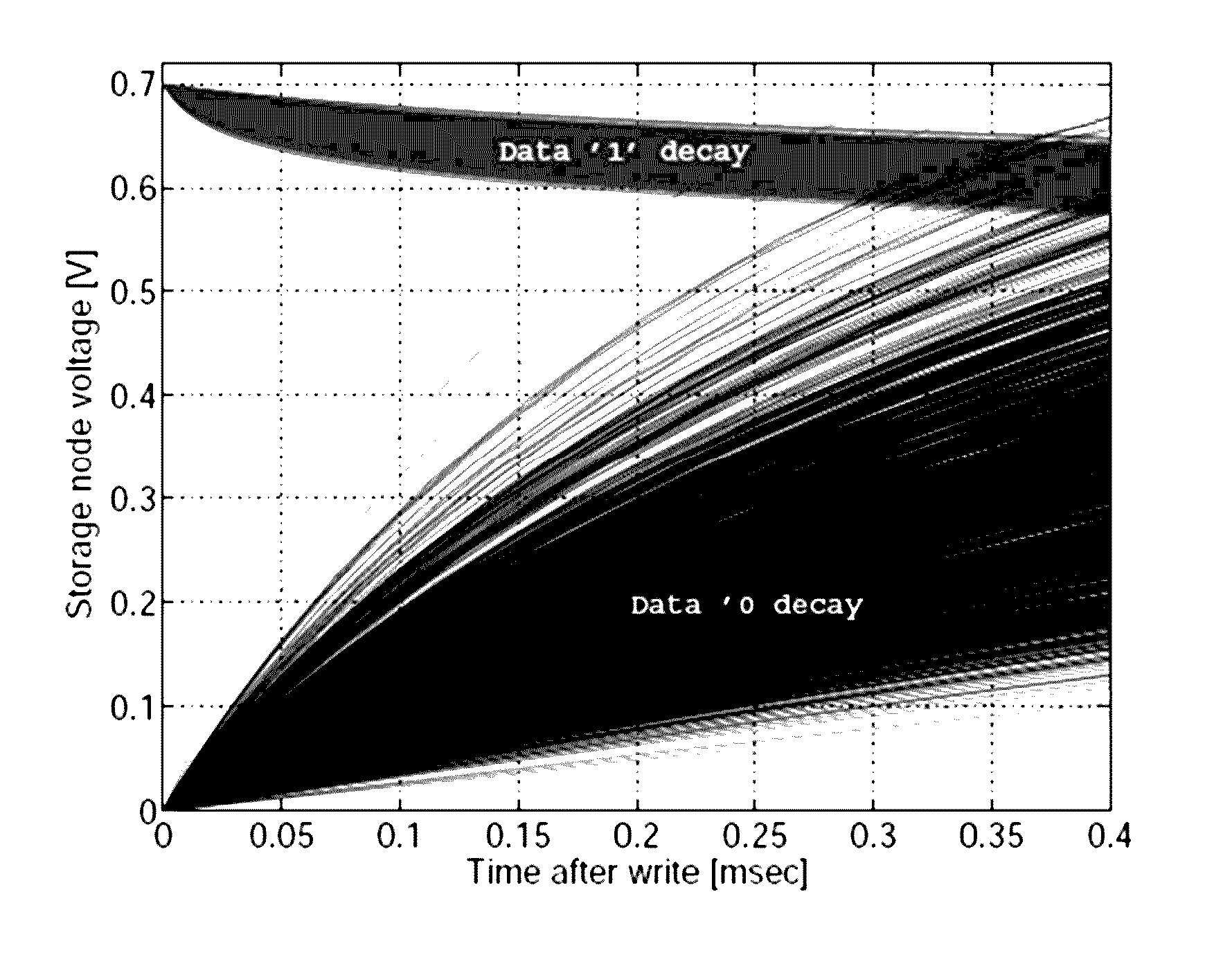
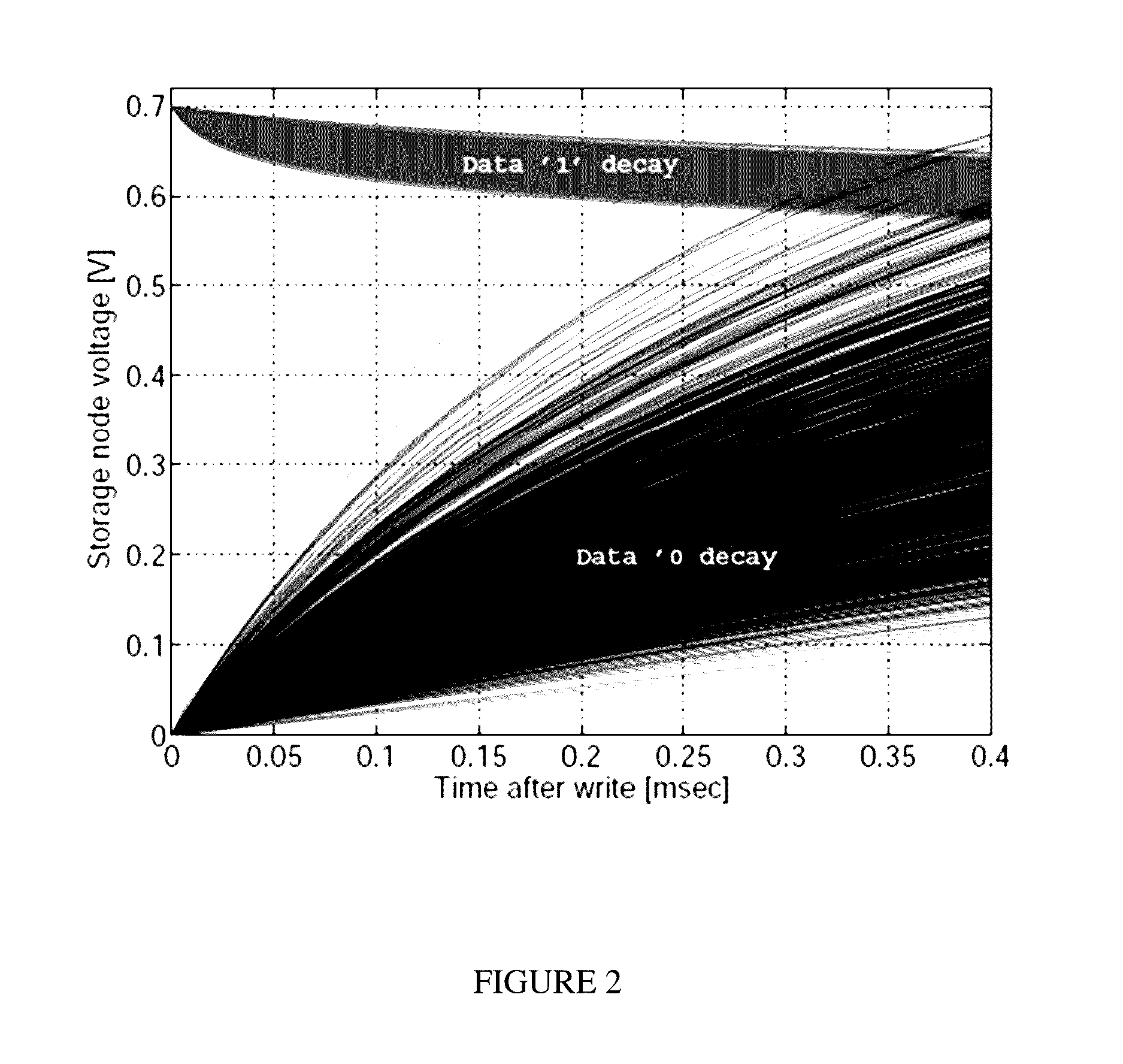
[0113]The simulation results presented below are for a 64×32 bit (2 kb) memory macro based on the 4T PMOS gain cell 500 of FIG. 5. The memory macro was designed in a low-power CMOS 65 nm process. All devices were implemented with standard VT transistors to provide logic process compatibility. The operating voltage was selected to be 700 mV in order to demonstrate compatibility with power-aware (near-threshold) applications.

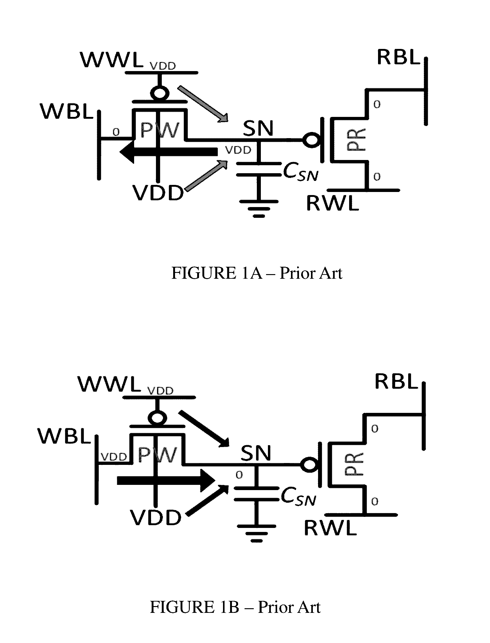
[0114]Reference is now made to FIG. 10 which is a timing diagram demonstrating 4T PMOS gain cell operation through subsequent write and read operations.

[0115]Initially, a ‘0’ is written to SN by pulsing WWL to a negative voltage (−700 mV), thereby discharging SN through WBL. Next, a read operation is performed by pre-discharging RBL by pulsing the PC control signal (not shown), and subsequently cha...


PUM


Abstract

A gain cell includes a write bit line input, a read bit line output, a write trigger input and a read trigger input. The gain cell also includes a write transistor, retention element and read transistor. Each of the transistors includes a respective first diffusion connection, gate connection and second diffusion connection. The write transistor first diffusion connection is connected to the write bit line input and the write transistor gate connection is connected to the write trigger input. The read transistor first diffusion connection being connected to the read bit line output and the second diffusion connection is connected to the read trigger input. The retention element buffers between write transistor and the read transistor during data retention. The retention element also connects or disconnects a write transistor diffusion connection to/from a constant voltage in accordance with a retained data level at the read transistor gate connection.

Description

FIELD AND BACKGROUND OF THE INVENTION[0001]The present invention, in some embodiments thereof, relates to a gain cell with internal feedback and, more particularly, but not exclusively, to a four-transistor gain cell with internal feedback.[0002]Modern microprocessors and other VLSI systems-on-chip (SoCs) implemented in aggressively scaled CMOS technologies are characterized by high leakage currents, and require an increasing amount of embedded memory [ref. 1]. Such embedded memory, typically implemented as 6-transistor (6T)-bitcell SRAM macrocells, not only consume an ever growing share of the total silicon area but also significantly contributes to the leakage power of the system. (The leakage power is a large share of the total power budget in deeply scaled CMOS nodes.) Unfortunately, besides several advantages like fast access speed and robust, static data retention, the 6T SRAM bitcell is relatively large, exhibits several leakage paths, and has dramatically increased failure r...

Claims


Application Information

Patent Timeline
IPC IPC(8): G11C7/10G11C5/06
CPCH01L27/1104G11C11/4097G11C11/412G11C5/06G11C5/025G11C7/10H01L27/11G11C11/403H10B10/00H10B10/12
Inventor GITERMAN, ROBERTTEMAN, ADAMMEINERZHAGEN, PASCALBURG, ANDREASFISH, ALEXANDER
Owner BAR ILAN UNIV
Why Eureka
Try Eureka