Lateral double-diffused transistor and manufacturing method thereof

A technology of lateral double diffusion and transistors, which is applied in semiconductor/solid-state device manufacturing, semiconductor devices, electrical components, etc., can solve the problems of NPN being easily turned on by mistake, difficulty in increasing breakdown voltage, and device function failure, so as to improve self-protection capability, expanding the effective lead-out area, and increasing the channel density

Active Publication Date: 2020-09-25
JOULWATT TECH INC LTD
View PDF6 Cites 0 Cited by
  • Summary
  • Abstract
  • Description
  • Claims
  • Application Information

AI Technical Summary

Problems solved by technology

In the application of LDMOS, it is required to reduce the source-drain on-resistance Rdson of the device as much as possible under the premise of satisfying the high source-drain breakdown voltage BV-dss, but the optimization requirements of source-drain breakdown voltage and on-resistance are indeed contradictory However, it is difficult to reduce the on-resistance and increase the breakdown voltage at the same time
[0003] LDMOS devices are usually used in the case of high current and high voltage. When the d

Method used


Image

  • Lateral double-diffused transistor and manufacturing method thereof
  • Lateral double-diffused transistor and manufacturing method thereof
  • Lateral double-diffused transistor and manufacturing method thereof

Examples


Embodiment Construction

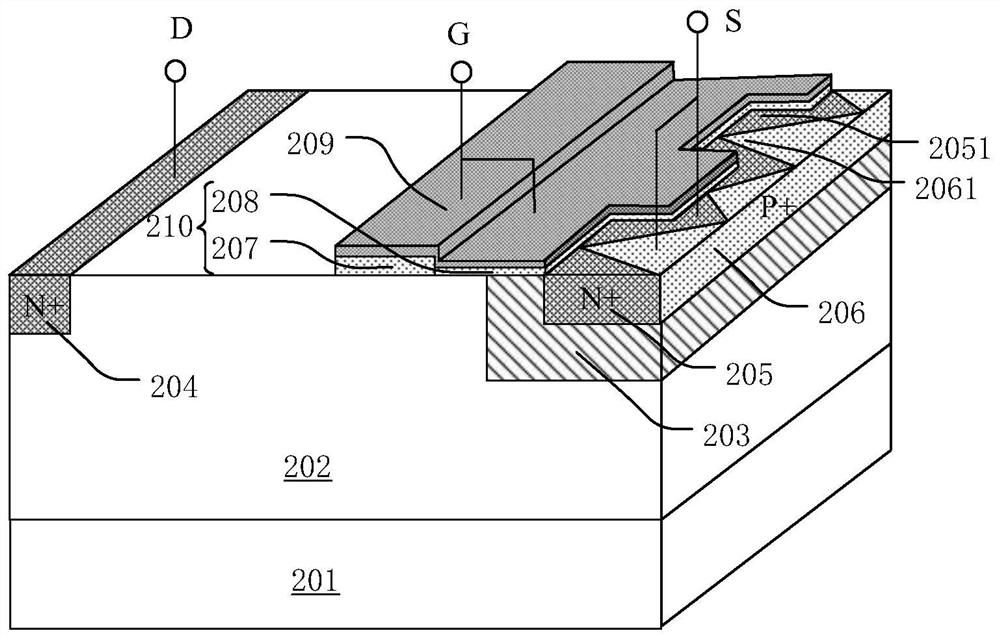
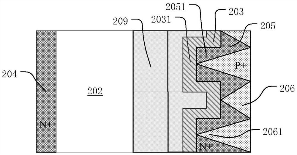
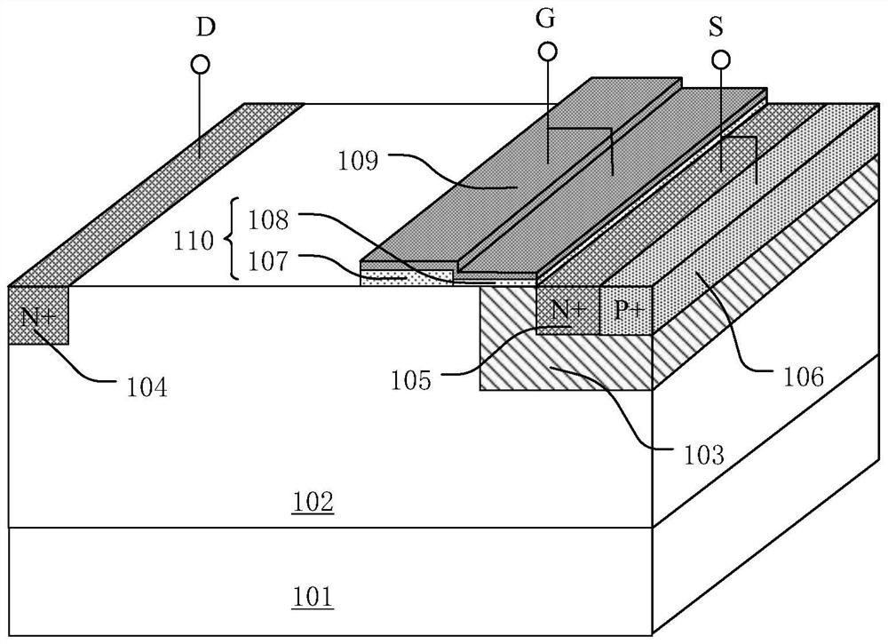
[0040] Various embodiments of the invention will be described in more detail below with reference to the accompanying drawings. In the various drawings, the same elements are denoted by the same or similar reference numerals. For the sake of clarity, various parts in the drawings have not been drawn to scale. Also, some well-known parts may not be shown. For the sake of simplicity, the semiconductor structure obtained after several steps can be described in one figure.

[0041] When describing the structure of a device, when a layer or a region is referred to as being "on" or "over" another layer or another region, it may refer to being directly above another layer or another region, or between it and Other layers or regions are also included between another layer and another region. And, if the device is turned over, the layer, one region, will be "below" or "beneath" the other layer, another region. If it is to describe the situation directly on another layer or another ...


PUM


Abstract

The invention discloses a lateral double-diffused transistor and a manufacturing method thereof. The lateral double-diffused transistor comprises: a substrate; a drift region located at the top of thesubstrate; a drain region and a body region respectively positioned on two opposite sides of the top of the drift region; a source region and a body contact region positioned in the body region and adjacent to each other; and a dielectric layer and a field plate layer sequentially stacked on the surface of the drift region, wherein the body region partially extends towards the direction of the drain region to form at least one body region extending region, the body region extending region and the drift region adjacent to the body region extending region are distributed in an interdigitated manner, the body contact region is located on the side, away from the drain region, in the body region, and the body contact region partially extends in the direction where the drain region is located to form a body contact region extending region. According to the lateral double-diffused transistor, the interdigital body region and the sawtooth-shaped body contact region are arranged, so that the channel density of the device is increased, the on resistance is reduced, the body region resistance can be effectively reduced, and parasitic NPN false opening is prevented.

Description

technical field [0001] The present invention relates to the technical field of semiconductors, in particular to a lateral double-diffused transistor and a manufacturing method thereof. Background technique [0002] As a type of power field effect transistor, lateral double-diffused MOS (Lateral Double-Diffused MOSFET, LDMOS) transistor has process compatibility, good thermal stability and frequency stability, high gain, low feedback capacitance and thermal resistance, and constant input impedance and other excellent properties, so it has been widely used. In the application of LDMOS, it is required to reduce the source-drain on-resistance Rdson of the device as much as possible under the premise of satisfying the high source-drain breakdown voltage BV-dss, but the optimization requirements of source-drain breakdown voltage and on-resistance are indeed contradictory However, it is difficult to reduce the on-resistance and increase the breakdown voltage at the same time. [...

Claims


Application Information

Patent Timeline
IPC IPC(8): H01L29/78H01L29/06H01L21/336
CPCH01L29/7816H01L29/0684H01L29/66681
Inventor 葛薇薇
Owner JOULWATT TECH INC LTD
Why Eureka
Try Eureka