Voltage regulator with dynamic charge pump control

a voltage regulator and dynamic charge technology, applied in the direction of instruments, power conversion systems, and apparatus without intermediate ac conversion, can solve the problems of large die area of charge pump blocks, and large amount of coupling to the regulator output, so as to minimize the glitches on the regulator output and minimize the glitches

Active Publication Date: 2017-03-02
VIDATRONIC
View PDF12 Cites 30 Cited by
  • Summary
  • Abstract
  • Description
  • Claims
  • Application Information

AI Technical Summary

Benefits of technology

[0010]In general, in one aspect, the invention relates to a novel architecture and method to significantly reduce the quiescent current of charge pump circuit blocks that drive cascode devices of voltage regulator circuits with NMOS pass devices by dynamically switching these charge pump blocks ON and OFF based on need, thus reducing its time-averaged current consumption. In accordance with some embodiments of the invention, an architecture and method to sense the charge pump voltage, compare it against a reference level that generates control signals to determine whether the charge pump circuits need to be ON or OFF during regulator operation.
[0015]In general, in one aspect, the invention relates to a novel architecture and method to significantly reduce the quiescent current of charge pump circuit blocks that drive voltage regulator circuits with NMOS pass devices by dynamically switching these charge pump blocks ON and OFF based on need, thus reducing its time-averaged current consumption. In accordance with some embodiments of the invention, an architecture and method to ensure that the charge pump drives only gates of transistors and no static current loads, so that the voltage may be preserved for long periods of time, before slowly draining due to leakage loads.
[0020]In general, in one aspect, the invention relates to a novel architecture and method to minimize glitches on the regulator output during initial start-up. In accordance with some embodiments of the invention, an architecture and method to start up the regulator using a clean start-up circuit that first charges the regulator output from OV up to the point where it reaches the final regulation set point voltage and then hands over control to the charge pump which then sustains the regulator output through the feedback loop action at the exact same set point. This process minimizes the glitches on the regulator output, as the transition from start-up to closed loop regulation happens at the same set point.

Problems solved by technology

However, all these schemes suffer from the drawback of higher quiescent current and larger die area for the charge pump blocks, as the charge pump block has to drive circuits that present quiescent load currents and also run all the time the regulator is in operation.
Specifically regarding the '670 and '916 applications, the charge pump switching noise / ripple occurs right at the gate of the pass transistor, thereby causing some amount of coupling to the regulator output.
Due to this reason, the pass transistor tends to be excessively large in size, as it has to withstand high voltage, in addition to having to sustain the full load current.
Use of such a charge pump, however is usually not preferred, as it comes with multiple limitations.
Not only does it take up significant extra die area due to large sized capacitors and big high voltage switch sizes required to sustain the load currents of (201) and (202) along with the leakage related charge losses of the parasitic transistors that are formed to the wells and substrates, but, it also requires significant amount of quiescent current to run itself, not to mention the additional power due to the associated oscillator and other support circuitry required to run the charge pump.
Typical charge pump circuits consume several hundreds of μA to mA, thereby significantly reducing the competitive aspect of the product and in several cases, rendering the resulting product un-usable.

Method used


Image

  • Voltage regulator with dynamic charge pump control
  • Voltage regulator with dynamic charge pump control
  • Voltage regulator with dynamic charge pump control

Examples


Embodiment Construction

[0032]Aspects of the present disclosure are shown in the above-identified drawings and are described below. In the description, like or identical reference numerals are used to identify common or similar elements. The drawings are not necessarily to scale and certain features may be shown exaggerated in scale or in schematic in the interest of clarity and conciseness.

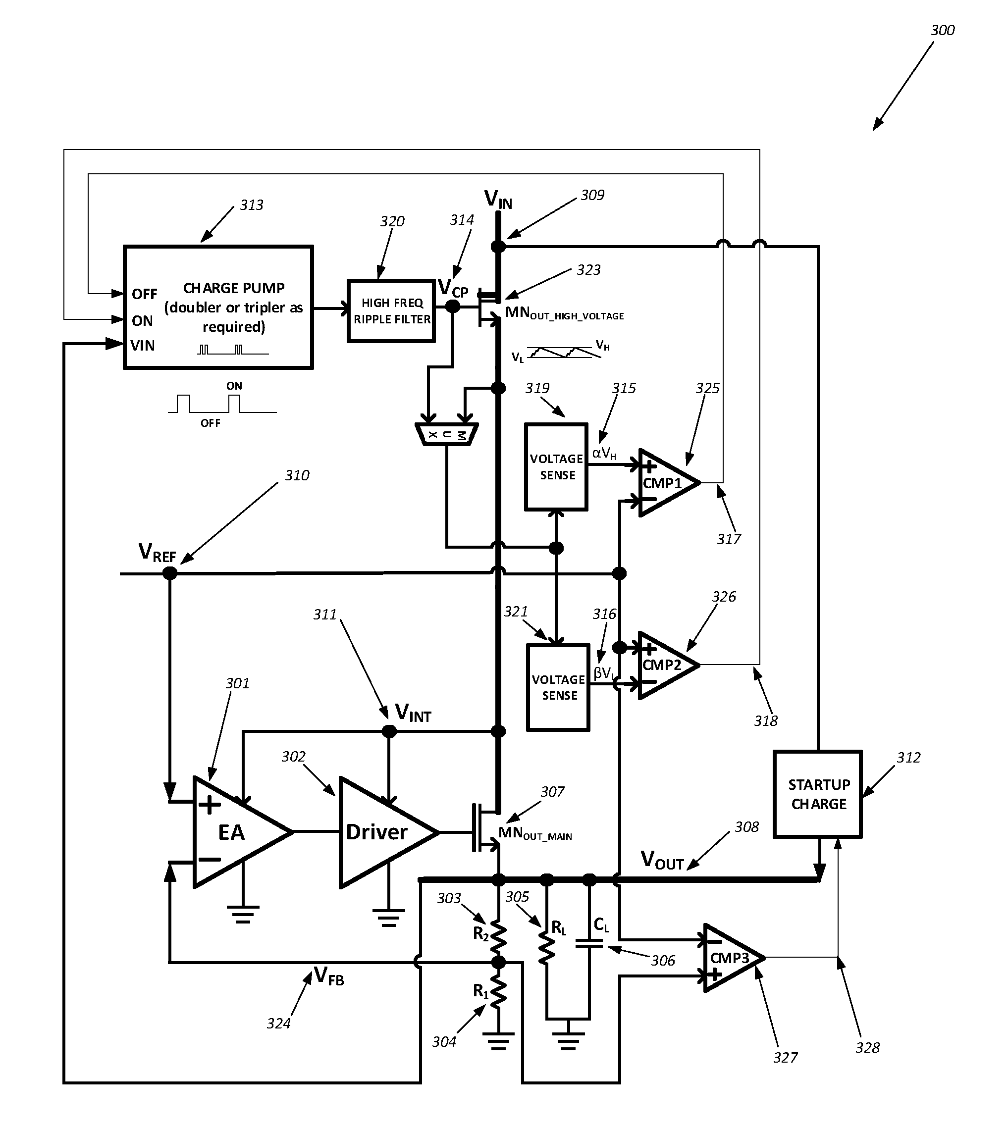
[0033]In accordance with embodiments of this patent, innovative solutions are provided which address the quiescent current problem by employing modified architectures that dynamically control the charge pumps and their associated circuits to keep them ON only when it is really required, while turning it OFF for significant chunks of time for which it is not needed

[0034]In accordance with embodiments of the invention, if it is desired to achieve low drop-out, in addition to low quiescent current, further innovations are proposed that use multiple input floating gate NMOS transistors as a pass device (1000) (FIG. 10), bia...


PUM


Abstract

A charge pump driven Linear Voltage Regulator (LVR) system with a cascoded n-type output pass device includes an error amplifier; a voltage feedback network; a dynamically controlled charge pump block that is ON only when required and OFF otherwise; a gate drive system configured to ensure that the charge pump drives only gate of a cascode transistor and no DC or static current load such that a voltage is preserved for a duration; and a filter at the charge pump output toreduce an impact of the switching noise of the charge pump on the regulator output, wherein the filter is outside a main servo loop of the regulator, wherein an n-type pass element and / or cascode element in the cascoded n-type output pass device comprises at least one of a Metal Oxide Semiconductor (MOS) Field Effect Transistor (FET), a bipolar junction transistor, an LDMOS, or a FinFET device.

Description

CROSS REFRENCE TO RELATED APPLICATIONS[0001]This claims the benefits of Provisional Application No. 62 / 211,356, filed on Aug. 28, 2015, the disclosure of which is incorporated by reference in its entirety.BACKGROUND[0002]FIG. 1 shows a schematic block diagram of a generic Linear Voltage Regulator (100), with its main components being the Error Amplifier (101), the Gate Driver (102), the feedback network consisting R2 (103) and R1 (104), the load network consisting of RL (105) and CL (106) and last, but certainly not the least, the pass device MPASS (107). The closed loop operation of the voltage regulator fixes the output voltage VOUT (108) to VOUT=VREF*(1+R2 / R1), by forcing the feedback node VFB (111) to be equal to the reference voltage VREF (110). It is interesting to note that the output voltage is independent of the Input Supply VIN (109). Throughout this description, the terms, “power / input supply,”“supply,”“VIN,” and “VIN terminal or node” may be used interchangeably to refer...

Claims


Application Information

Patent Timeline
Patent Type & Authority Applications(United States)
IPC IPC(8): H02M3/07
CPCH02M3/07G05F1/575H02M1/0045G05F1/56
Inventor RAGHUPATHY, ANAND VEERAVALLI
Owner VIDATRONIC
Why Eureka
Try Eureka