Semiconductor device

Active Publication Date: 2017-03-23
FUJI ELECTRIC CO LTD
View PDF2 Cites 8 Cited by
  • Summary
  • Abstract
  • Description
  • Claims
  • Application Information

AI Technical Summary

Benefits of technology

[0022]According to one aspect of the present invention, semiconductor device includes a semiconductor substrate of a first conductivity type, formed of a silicon carbide semiconductor; an active region disposed on a front surface of the semiconductor substrate and through which main current flows; and an edge termination structure portion surrounding a periphery of the active region. The edge termination structure portion has: plural semiconductor regions of a second conductivity type, disposed concentrically surrounding the periphery of the active region, the farther outward a semiconductor region thereamong is arranged, the lower an impurity concentration thereof is, and an intermediate region of the second conductivity type, disposed so as to mutually contact one combination of the semiconductor regions that are adjacent, the intermediate region having an impurity concentration th

Problems solved by technology

In the case of the silicon carbide semiconductor device having an extremely small thermal diffusion of impurities and subjected to ion implantation with high acceleration voltage for introducing impurities, it is difficult to apply the VLD structure to reduce the impurity concentration of the p−-type low-concentration region in the outward direction f

Method used


Image

  • Semiconductor device
  • Semiconductor device
  • Semiconductor device

Examples


first embodiment

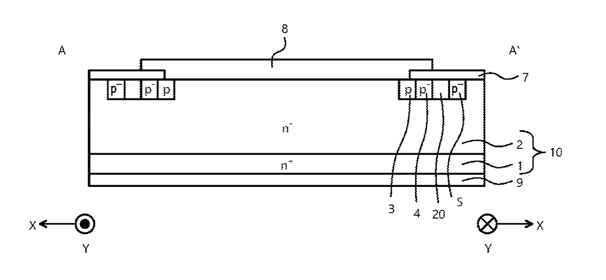
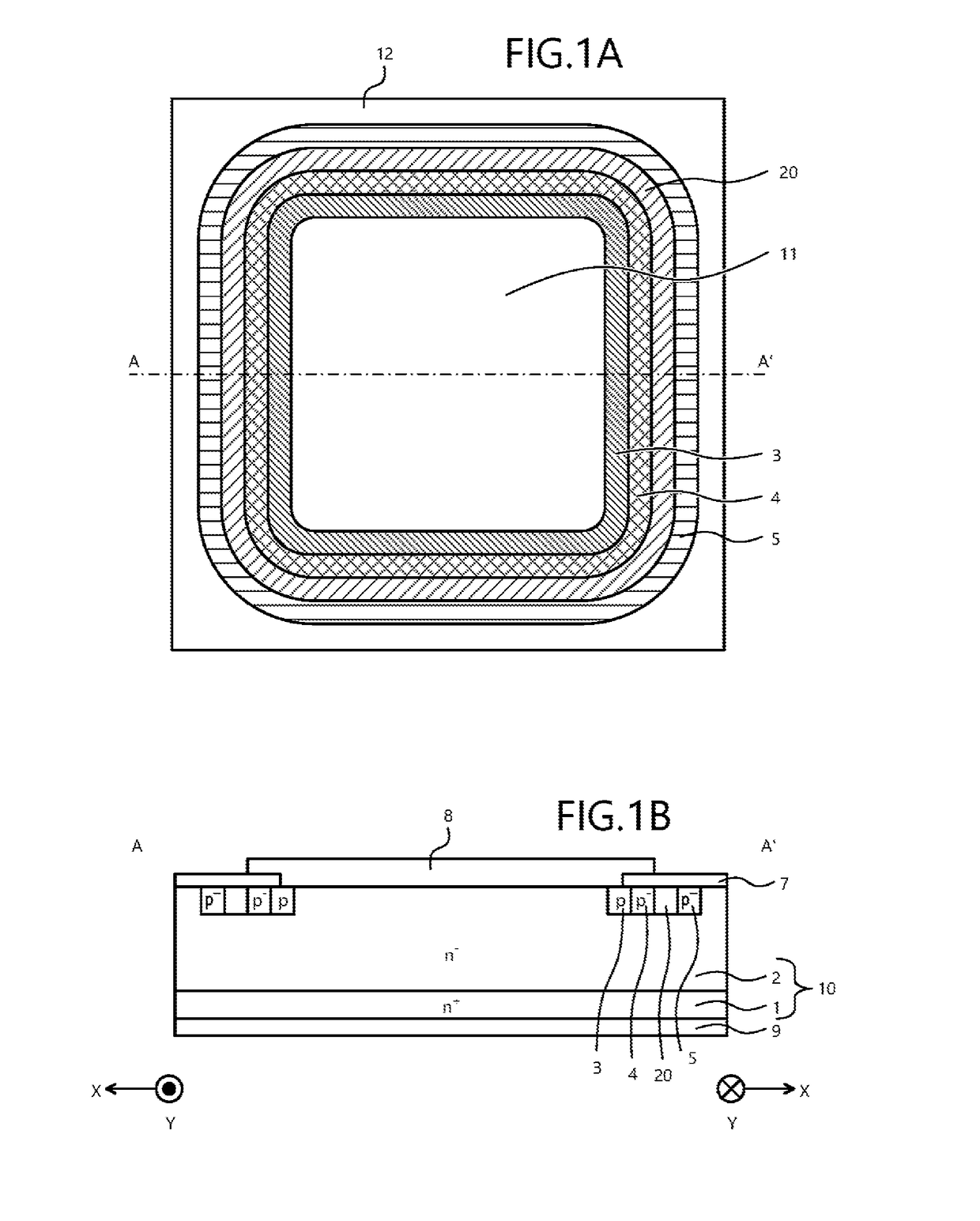
[0109]As shown in FIG. 1A, the semiconductor device includes an active region 11 through which current flows in an on-state, and an edge termination structure portion 12 relaxing an electric field on a base front surface side of the active region 11 to retain a breakdown voltage. The active region 11 is provided with a device structure (not depicted) of the SBD. On a boundary between the active region 11 and the edge termination structure portion 12, a p-type guard ring 3 is disposed to surround a periphery of the active region 11. The edge termination structure portion 12 surrounds the periphery of the active region 11. The edge termination structure portion 12 is provided with a JTE structure made up of two p-type regions (semiconductor regions of a second-conductivity type (a p−-type region 4 and a p−−-type region 5)) having differing impurity concentrations and the p-type electric field relaxation region (an intermediate region of the second-conductivity type) 20 disposed betwe...

seventh embodiment

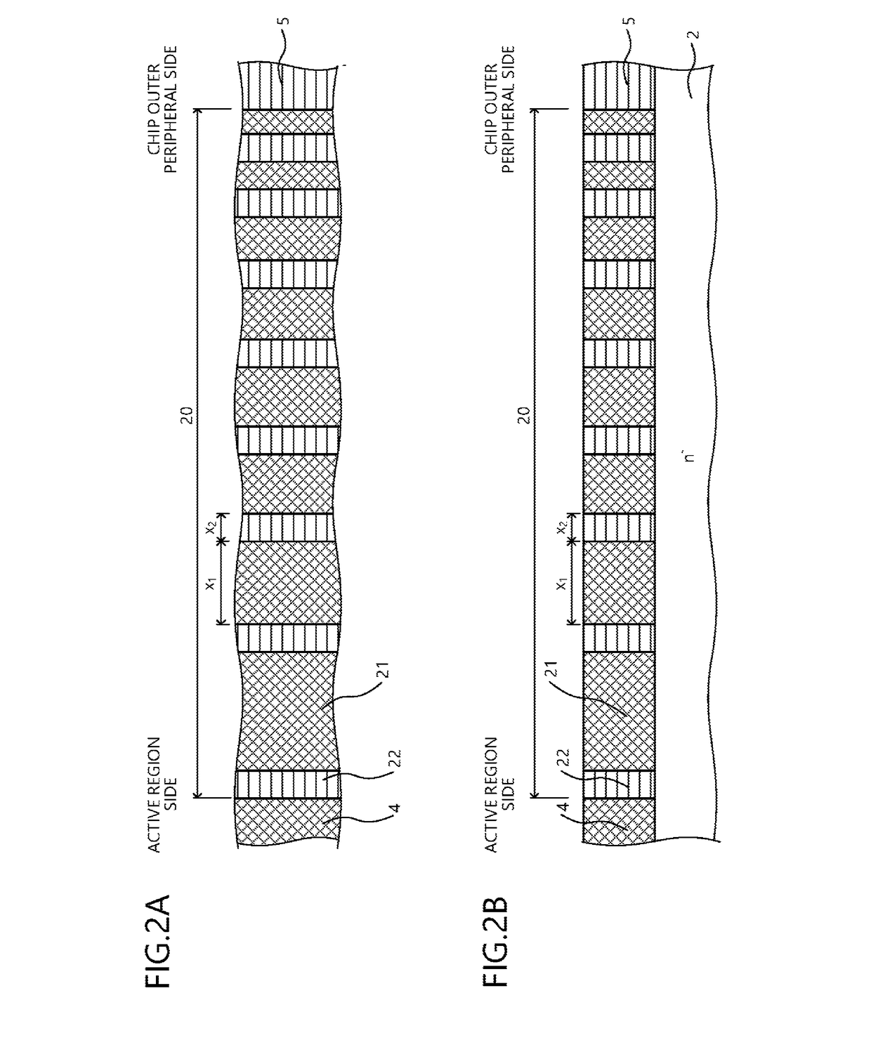
[0186]The second difference is that the average impurity concentration differences ΔNp between adjacent sections 71 to 78 is equal. As described above, the widths Δx of the sections 71 to 78 are all equal, whereby the average impurity concentration slope 70a (decreasing ratio of the average impurity concentration in direction from inner side toward outside=ΔNp / Δx) of the electric field relaxation region 20 decreasing from the inner side toward the outside is constant across the entire electric field relaxation region 20 (i.e., all of the sections 71 to 78). In FIG. 31C, an approximated straight line representing the average impurity concentration slope 70a of the electric field relaxation region 20 is indicated by a dotted line (similarly in FIGS. 34C, 46B, and 47B. In each of the sections 71 to 78, similar to the seventh embodiment, one or more of the equivalent concentration regions 30 of the same conditions is arranged. Therefore, the average impurity concentrations of each of th...

third embodiment

[0219]In particular, the second subregion portions 32 having an impurity concentration that is higher than that of the second subregions 22 are selectively disposed at a predetermined interval along the tangential direction Y in all of the second subregions 22 arranged in the first section 71 innermost in the electric field relaxation region 20. In other words, the first subregion 21 and the fourth subregion 20b configured by the second subregion 22 and the second subregion portions 32 are alternately and repeatedly arranged along the normal direction X in the first section 71 innermost in the electric field relaxation region 20 and one of more of the equivalent concentration regions 30b made up of one combination of a fourth subregion 20b and adjacent first subregion 21 are cyclically arranged. Thus, similar to the third embodiment, the p-type impurity concentration difference Δnph of the first JTE region 4 and the first section 71 (the equivalent concentration region 30b) innermos...


PUM


Abstract

In an edge termination structure portion, first and second JTE regions are disposed concentrically surrounding an active region. Between the first and second JTE regions, a p-type electric field relaxation region is disposed that includes a first subregion and a second subregion alternately and repeatedly arranged concentrically surround a periphery of the first JTE region. An average impurity concentration of the electric field relaxation region is higher that the impurity concentration of the first JTE region adjacent on the inner side and lower than the impurity concentration of the second JTE region adjacent on the outer side. First subregions have widths that decrease the farther outward they are arranged. Second subregions have widths that are substantially the same independent of position. The first subregions and the first JTE region have equal impurity concentrations. The second subregions and the second JTE region have equal impurity concentrations.

Description

CROSS REFERENCE TO RELATED APPLICATIONS[0001]This is a continuation application of International Application PCT / JP2015 / 076369 filed on Sep. 16, 2015 which claims priority from Japanese Patent Application Nos. 2014-263509 filed on Dec. 25, 2014, and 2015-122451 filed on Jun. 17, 2015 the contents of which are incorporated herein by reference.BACKGROUND OF THE INVENTION[0002]1. Field of the Invention[0003]The embodiments discussed herein relate to a semiconductor device.[0004]2. Description of the Related Art[0005]Semiconductor devices using a silicon carbide (SiC) semiconductor (hereinafter referred to as a silicon carbide semiconductor device) are recently attracting attention as devices that exceed the limitations of semiconductor devices using a silicon (Si) semiconductor material. In particular, silicon carbide semiconductor devices are expected to be applied to high voltage devices by taking advantage of characteristics of higher critical field strength and higher thermal condu...

Claims


Application Information

Patent Timeline
IPC IPC(8): H01L29/16H01L29/36H01L29/872H01L29/06
CPCH01L29/1608H01L29/872H01L29/36H01L29/0619H01L21/0465H01L29/0615H01L29/6606H01L29/0623H01L29/8611
Inventor KITAMURA, SHOJI
Owner FUJI ELECTRIC CO LTD
Why Eureka
Try Eureka