Method of manufacturing semiconductor device and non-transitory computer-readable recording medium

Active Publication Date: 2017-03-30
KOKUSA ELECTRIC CO LTD
View PDF1 Cites 1 Cited by
  • Summary
  • Abstract
  • Description
  • Claims
  • Application Information

AI Technical Summary

Benefits of technology

[0011]A technique is provided in which an oxide layer whose thickness and resistivity (sheet resistance) are arbitrarily controlled is formed with excellent uniformity

Problems solved by technology

These structures have a problem that when a metal film (e.g., a TiN film) which is a bottom electrode is formed and then a high-k film or the like is further formed as a capacitive film, a surface of the metal film is strongly oxidized by

Method used


Image

  • Method of manufacturing semiconductor device and non-transitory computer-readable recording medium
  • Method of manufacturing semiconductor device and non-transitory computer-readable recording medium
  • Method of manufacturing semiconductor device and non-transitory computer-readable recording medium

Examples


Embodiment Construction

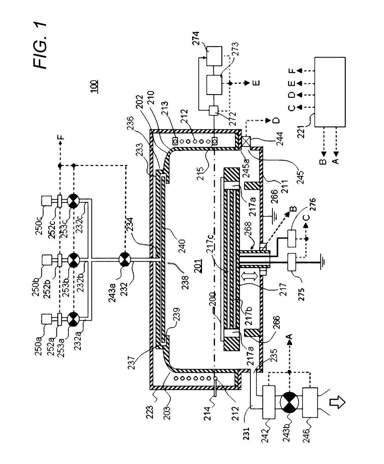
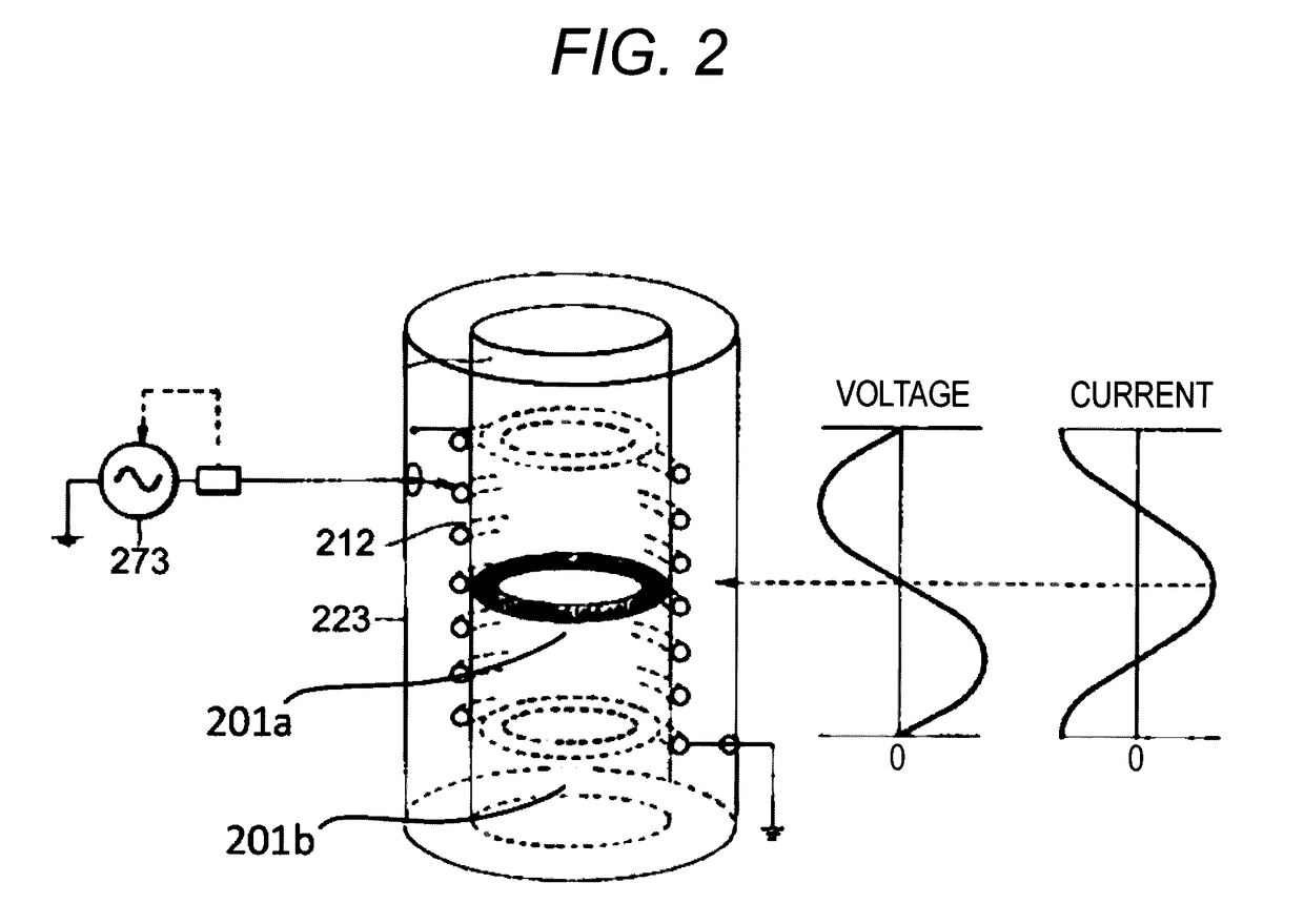
[0021](1) Configuration of a Substrate Processing Apparatus

[0022]A substrate processing apparatus according to a first embodiment will be described below using FIGS. 1 to 6.

[0023](Processing Chamber)

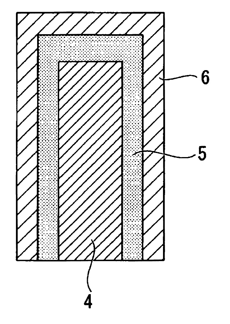
[0024]A processing apparatus 100 includes a processing furnace 202 where a wafer 200 is subjected to plasma processing. The processing furnace 202 is provided with a processing container 203 that forms a processing chamber 201. The processing container 203 includes a dome-shaped top container 210 which is a first container; and a dish-shaped bottom container 211 which is a second container. By the top container 210 placed over the bottom container 211, the processing chamber 201 is formed. The top container 210 is formed of, for example, a non-metallic material such as aluminum oxide (Al2O3) or quartz (SiO2), and the bottom container 211 is formed of, for example, aluminum (Al).

[0025]In addition, the bottom container 211 has a gate valve 244 provided at a lower sidewall thereof. When the...


PUM


Abstract

A semiconductor manufacturing method includes preparing a substrate having a metal film formed on a surface thereof; forming an oxide layer by oxidizing a surface of the metal film by plasma of a mixed gas of an oxygen-containing gas and a hydrogen-containing gas; and forming a thin film on the oxide layer by supplying at least an oxidizing gas to the substrate.

Description

BACKGROUND[0001]Technical Field[0002]The present invention relates to a method of manufacturing a semiconductor device and to a non-transitory computer-readable recording medium.[0003]Related Art[0004]With an increase in the density and performance of a semiconductor device, a capacitor process for a DRAM which is a semiconductor device has become a high aspect ratio to secure capacitance. In addition, in order to prevent a high cylindrical structure from collapsing, a structure where a top portion of a cylinder is supported has become common. These structures have a problem that when a metal film (e.g., a TiN film) which is a bottom electrode is formed and then a high-k film or the like is further formed as a capacitive film, a surface of the metal film is strongly oxidized by an oxidant such as ozone or H2O which is used to form the capacitive film.SUMMARY[0005]Due to the above-described problem, in recent years, a technique has been used in which a barrier layer is formed by oxid...

Claims


Application Information

Patent Timeline
IPC IPC(8): H01L27/108H01L21/02
CPCH01L27/1085H01L21/02244H01L21/02175H01L21/02252H01L21/02247H01J37/32926H01L21/67109H01L21/67757H01L21/68742H01L21/02186H01L21/02189H01L21/0228H01L21/02304H01L21/321H01L28/40H10B12/03
Inventor NAKAYAMA, MASANORIIGAWA, HIROTO
Owner KOKUSA ELECTRIC CO LTD
Why Eureka
Try Eureka