Base-attached encapsulant for semiconductor encapsulation, method for manufacturing base-attached encapsulant for semiconductor encapsulation, and method for manufacturing semiconductor apparatus

a technology of base-attached encapsulants and semiconductors, which is applied in the field of encapsulants, can solve the problems of semiconductor devices being detached from the substrate, substrate or wafer warp, and large hindrance, and achieves excellent handling ability, low cost, and improved laser marking properties.

Inactive Publication Date: 2017-04-06
SHIN ETSU CHEM IND CO LTD
View PDF4 Cites 2 Cited by
  • Summary
  • Abstract
  • Description
  • Claims
  • Application Information

AI Technical Summary

Benefits of technology

[0047]By using a thermosetting resin composition which contains such an amount of colorant, it is possible to achieve better appearance and laser marking property.
[0048]As described above, the inventive base-attached encapsulant for semiconductor encapsulation achieves low cost and excellent handling ability, can suppress warpage and fall-off of semiconductor devices from the substrate even when encapsulating a large-area substrate with thin thickness, has excellent encapsulating properties such as heat resistance and moisture resistance reliability, and can manufacture a semiconductor apparatus having good appearance and laser marking property. Moreover, the inventive manufacturing method can easily manufacture such a base-attached encapsulant for semiconductor encapsulation.

Problems solved by technology

When encapsulating a large-diameter substrate having semiconductor devices mounted thereon or a large-diameter wafer having semiconductor devices formed thereon with a diameter of 300 mm (12 inches) or more, however, there has been a big problem that the substrate or the wafer warps due to shrinkage stress of the encapsulating resin such as epoxy resin, at the time of encapsulating and curing.
In addition, when the device-mounted surface of the large-diameter substrate on which semiconductor devices have been mounted is encapsulated on a wafer level, there arises a problem that the semiconductor devices are detached from the substrate made of a metal, etc. by shrinkage stress of the encapsulating resin at the time of encapsulating and curing.
These problems have been large hindrance to mass-production of semiconductor apparatuses by collective encapsulation.
A semiconductor apparatus encapsulated by using the above base-attached encapsulant for semiconductor encapsulation bears the surface of the base, and accordingly the appearance gets worse compared to a semiconductor apparatus encapsulated with a conventional thermosetting epoxy resin etc., and there arises a problem that the laser marking property is damaged.
However, by forming the surface resin layer onto the surface of the base, the base is liable to generate warpage due to the difference of the thermal expansion coefficient between the base and the surface resin layer, and accordingly it can be difficult to form an encapsulating resin layer onto the surface of the base.
Moreover, there has been a problem of worsening the handling ability of the base-attached encapsulant for semiconductor encapsulation itself such as remaining of warpage of the base even after forming an encapsulating resin layer.
Furthermore, there has been a problem that the producing cost increases due to an addition of a step for forming the surface resin layer.

Method used


Image

  • Base-attached encapsulant for semiconductor encapsulation, method for manufacturing base-attached encapsulant for semiconductor encapsulation, and method for manufacturing semiconductor apparatus
  • Base-attached encapsulant for semiconductor encapsulation, method for manufacturing base-attached encapsulant for semiconductor encapsulation, and method for manufacturing semiconductor apparatus
  • Base-attached encapsulant for semiconductor encapsulation, method for manufacturing base-attached encapsulant for semiconductor encapsulation, and method for manufacturing semiconductor apparatus

Examples


example 1

Preparation of Resin Composition for Producing Base

[0147]Into 60 parts by mass of a cresol novolac type epoxy resin, 30 parts by mass of a phenol novolac resin, and 0.6 part by mass of a catalyst TPP (triphenylphosphine), 300 parts by mass of toluene was added. This was stirred and mixed to prepare a toluene dispersion of an epoxy resin composition.

[0148]To this toluene dispersion of an epoxy resin composition, E-glass cloth (manufactured by Nitto Boseki co., Ltd., thickness: 50 μm) as a fibrous base was dipped to impregnate the E-glass cloth with the toluene dispersion of the epoxy resin composition. The glass cloth was passed through a roll with the gap adjusted to 75 μm, and then left for 15 minutes at 120° C. to volatilize toluene. The glass cloth was subjected to heat molding at 175° C. for 5 minutes to obtain a molded article. This was subjected to heating at 180° C. for 4 hours (post cure) to cure the impregnated thermosetting resin composition, thereby obtaining an epoxy res...

example 2

Preparation of Resin Composition for Producing Base

[0153]Into 60 parts by mass of a cresol novolac type epoxy resin, 30 parts by mass of a phenol novolac resin, 3 parts by mass of titanium black as a black pigment, and 0.6 part by mass of a catalyst TPP, 300 parts by mass of toluene was added. This was stirred and mixed to prepare a toluene dispersion of an epoxy resin composition.

[0154]To this toluene dispersion of an epoxy resin composition, E-glass cloth (manufactured by Nitto Boseki co., Ltd., thickness: 50 m) as a fibrous base was dipped to impregnate the E-glass cloth with the toluene dispersion of the epoxy resin composition. The glass cloth was passed through a roll with the gap adjusted to 75 μm, and then left for 15 minutes at 120° C. to volatilize toluene. The glass cloth was subjected to heat molding at 175° C. for 5 minutes to obtain a molded article. This was subjected to heating at 180° C. for 4 hours (post cure) to cure the impregnated thermosetting resin composition...

example 3

Preparation of Resin Composition for Producing Base

[0159]Into 50 parts by mass of dimethylpolysiloxane both molecular terminals of which were blocked with vinyl groups as an organosilicon compound having a nonconjugated unsaturated bond, 50 parts by mass of dimethylpolysiloxane both molecular terminals of which were blocked with dimethylhydrogensiloxy groups, 0.2 part by mass of acetylene alcohol-based ethynylcyclohexanol as a reaction inhibitor, 0.1 part by mass of an octyl alcohol-modified solution of a chloroplatinic acid, and 3 parts by mass of carbon black as a black pigment, 200 parts by mass of toluene was added. This was stirred and mixed to prepare a toluene dispersion of a silicone resin composition.

[0160]To this toluene dispersion of a silicone resin composition, E-glass cloth (manufactured by Nitto Boseki co., Ltd., thickness: 50 μm) as a fibrous base was dipped to impregnate the E-glass cloth with the toluene dispersion of the silicone resin composition. The glass cloth...


PUM

PropertyMeasurementUnit
thickness Tbaaaaaaaaaa
diameteraaaaaaaaaa
diameteraaaaaaaaaa

Abstract

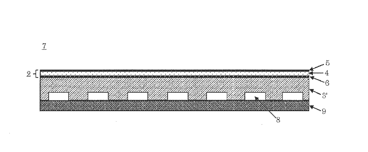
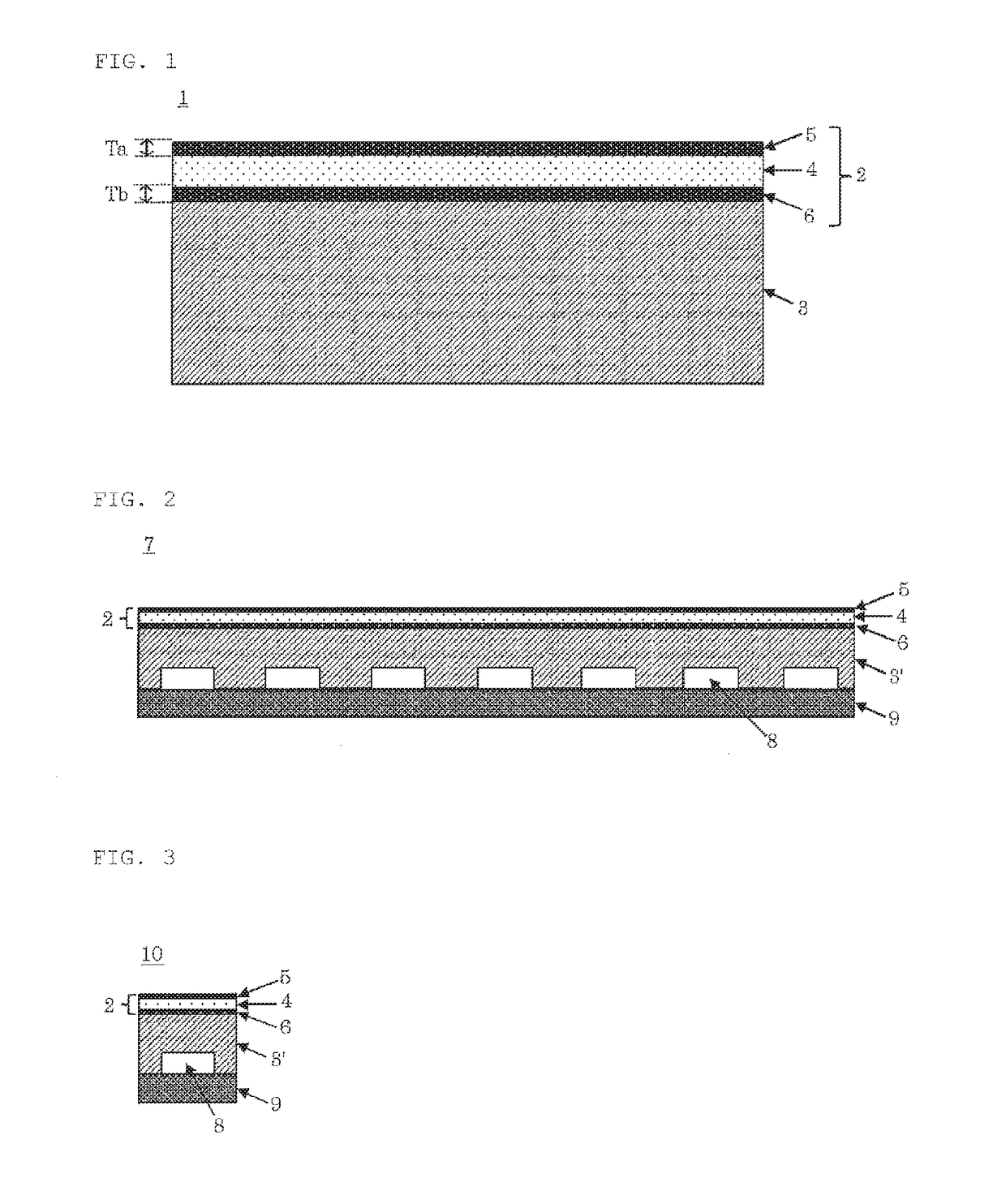
A base-attached encapsulant for semiconductor encapsulation, includes a base and encapsulating resin layer on one surface of the base, the base being composed of a fibrous base layer in which a thermosetting resin composition containing a thermosetting resin is impregnated into a fibrous base and cured, a cured material layer A composed of a cured material of the thermosetting resin composition formed on the fibrous base layer at the opposite side to the encapsulating resin layer, and a cured material layer B composed of a cured material of the thermosetting resin composition formed on the fibrous base layer at the encapsulating resin layer side. The thickness Ta of the cured material layer A is 0.5 μm or more. The ratio Ta/Tb of the thickness Ta of the cured material layer A and the thickness Tb of the cured material layer B is in a range of 0.1 to 10.

Description

BACKGROUND OF THE INVENTION[0001]Field of the Invention[0002]The present invention relates to an encapsulant capable of collectively encapsulating a device-mounted surface of a substrate on which semiconductor devices have been mounted, or a device-formed surface of a wafer on which semiconductor devices have been formed on a wafer level, particularly to a base-attached encapsulant for semiconductor encapsulation, a method for manufacturing the base-attached encapsulant for semiconductor encapsulation, and a method for manufacturing a semiconductor apparatus by using the base-attached encapsulant for semiconductor encapsulation.[0003]Description of the Related Art[0004]Various methods have heretofore been proposed and investigated about encapsulation, on a wafer level, of a device-mounted surface of a substrate on which semiconductor devices have been mounted or a device-formed surface of a wafer on which semiconductor devices have been formed, and there may be exemplified by a meth...

Claims


Application Information

Patent Timeline
Patent Type & Authority Applications(United States)
IPC IPC(8): H01L21/56H01L23/29H01L21/48H01L23/31
CPCH01L21/561H01L21/565H01L21/481H01L23/29H01L23/3135H01L23/562H01L2224/16227H01L2224/97H01L2224/16245H01L2924/3511H01L2223/54486H01L23/544H01L2224/81H01L23/3121H01L23/296B32B2260/046B32B2260/021
Inventor NAKAMURA, TOMOAKIAKIBA, HIDEKISHIOBARA, TOSHIOYAMAGUCHI, SHINSUKE
Owner SHIN ETSU CHEM IND CO LTD
Why Eureka
Try Eureka