Methods and Apparatus for Simulating Interaction of Radiation with Structures, Metrology Methods and Apparatus, Device Manufacturing Method

Active Publication Date: 2017-04-13
ASML NETHERLANDS BV
View PDF30 Cites 14 Cited by
  • Summary
  • Abstract
  • Description
  • Claims
  • Application Information

AI Technical Summary

Benefits of technology

[0009]The invention aims to allow simulation of interactions of radiation with microscopic structures by a more economical and/or robust method. The inventors have recognized that a new formulation of a modal method such as FMM (RCWA) can be devised, which is adapted to allow a fast, semi-

Problems solved by technology

On the other hand, reconstruction requires a great deal of computation.
Since this product can easily reach a factor of 1000, the computation might become e

Method used


Image

  • Methods and Apparatus for Simulating Interaction of Radiation with Structures, Metrology Methods and Apparatus, Device Manufacturing Method
  • Methods and Apparatus for Simulating Interaction of Radiation with Structures, Metrology Methods and Apparatus, Device Manufacturing Method
  • Methods and Apparatus for Simulating Interaction of Radiation with Structures, Metrology Methods and Apparatus, Device Manufacturing Method

Examples


Embodiment Construction

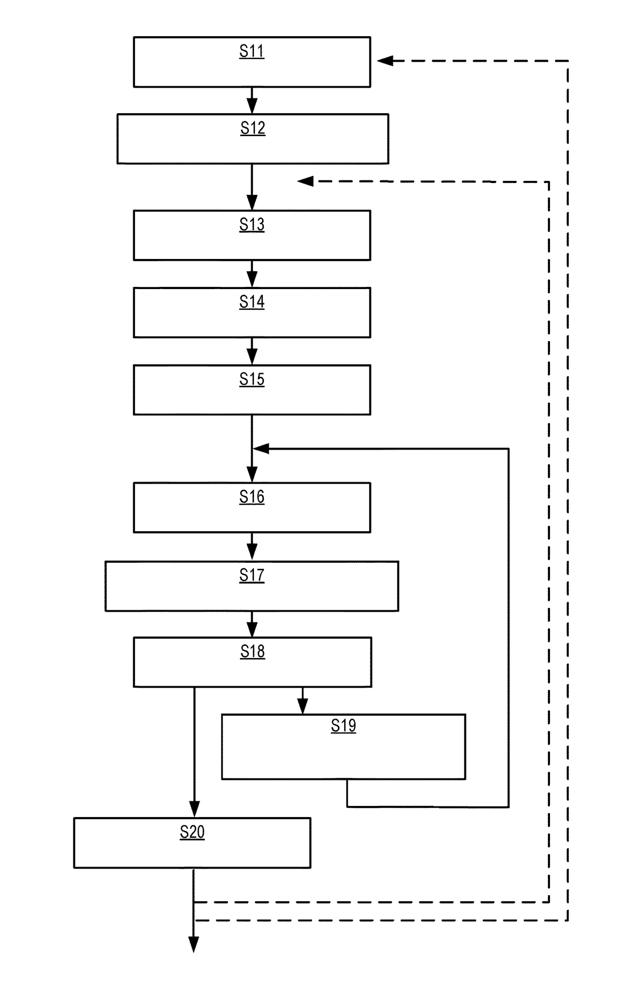
[0037]Before describing embodiments of the invention in detail, it is instructive to present an example environment in which embodiments of the present invention may be implemented.

Lithographic Manufacturing Background

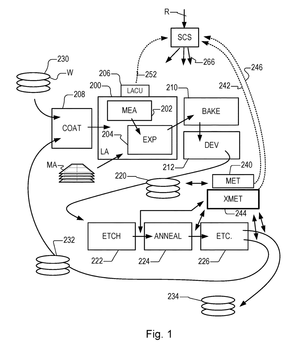
[0038]FIG. 1 at 200 shows a lithographic apparatus LA as part of an industrial facility implementing a high-volume, lithographic manufacturing process. In the present example, the manufacturing process is adapted for the manufacture of for semiconductor products (integrated circuits) on substrates such as semiconductor wafers. The skilled person will appreciate that a wide variety of products can be manufactured by processing different types of substrates in variants of this process. The production of semiconductor products is used purely as an example which has great commercial significance today.

[0039]Within the lithographic apparatus (or “litho tool”200 for short), a measurement station MEA is shown at 202 and an exposure station EXP is shown at 204. A control unit ...


PUM


Abstract

A structure of interest is irradiated with radiation for example in the x-ray or EUV waveband, and scattered radiation is detected by a detector (306). A processor (308) calculates a property such as linewidth (CD) by simulating interaction of radiation with a structure and comparing the simulated interaction with the detected radiation. A layered structure model (600, 610) is used to represent the structure in a numerical method. The structure model defines for each layer of the structure a homogeneous background permittivity and for at least one layer a non-homogeneous contrast permittivity. The method uses Maxwell's equation in Born approximation, whereby a product of the contrast permittivity and the total field is approximated by a product of the contrast permittivity and the background field. A computation complexity is reduced by several orders of magnitude compared with known methods.

Description

FIELD[0001]The present invention relates to methods and apparatus for simulating interaction of radiation with structures. The invention may be applied for example in metrology of microscopic structures, for example to assess and improve performance of a lithographic, or to determine the structure of a molecule or crystal. The radiation may be electromagnetic radiation of any desired wavelength, but the invention may find particular application in x-ray and so-called soft x-ray (extreme ultraviolet) wavebands.BACKGROUND[0002]While the invention may be applied to a range of applications, consider as an example the manufacture of integrated circuits (ICs) by a lithographic process. In that instance, a lithographic apparatus is used to apply a pattern of device features to be formed on an individual layer of the IC. This pattern can be transferred onto a target portion (e.g., including part of, one, or several dies) on a substrate (e.g., a silicon wafer).[0003]In lithographic processes...

Claims


Application Information

Patent Timeline
IPC IPC(8): G03F7/20G01B15/00G01N23/201
CPCG03F7/70625G01N2223/501G01B15/00G01N23/201G03F7/705
Inventor PISARENCO, MAXIMQUINTANILHA, RICHARDVAN KRAAIJ, MARKUS GERARDUS MARTINUS MARIA
Owner ASML NETHERLANDS BV
Why Eureka
Try Eureka