Optimized CMOS Analog Switch

a cmos analog switch and optical technology, applied in the field of optical optical cmos analog switches, can solve the problems of affecting image quality, double parasitic capacitance, and large on-resistance/parasitic capacitance trade-off, and achieve the effect of increasing parasitic capacitan

Active Publication Date: 2017-04-13
MICROCHIP TECH INC
View PDF0 Cites 13 Cited by
  • Summary
  • Abstract
  • Description
  • Claims
  • Application Information

AI Technical Summary

Benefits of technology

[0015]The preferred embodiment is a high-voltage CMOS switch circuit topology that reduces the on-resistance to 4-8 Ohms, which is an improvement by a factor of 2 to 4 without increasing the parasitic capacitance compared to the prior art. The circuit topology is straightforward to implement and is suitable for constructing, for example, a 4:1 ultrasound multiplexer (such as multiplexor 270) that can handle analog signals of ±100 V. The power supplies to this circuit are ±6 V and the control inputs are voltage levels of 0 and +5 V, compatible with standard CMOS circuits. The circuit is particularly useful in driving high-voltage transducers for ultrasound elastography probes.

Problems solved by technology

However, two switches connected in parallel also double the parasitic capacitance and affect the image quality.
The high-voltage capability of the devices further worsens the on-resistance / parasitic capacitance trade-off.
Fixed gate bias over the varying source voltage makes the on-resistance for positive signal much larger than that for negative signal and introduces second harmonic distortion.
Piezoelectric devices exhibit nonlinear behavior when subjected to high electric field.
Once the piezoelectric material is operating in nonlinear mode, the material likely is already damaged.
Thus, terminating a piezoelectric transducer with a high voltage is destructive to the piezoelectric material.
However, T-switch 600 experiences substantial heat dissipation.

Method used


Image

  • Optimized CMOS Analog Switch
  • Optimized CMOS Analog Switch
  • Optimized CMOS Analog Switch

Examples


Embodiment Construction

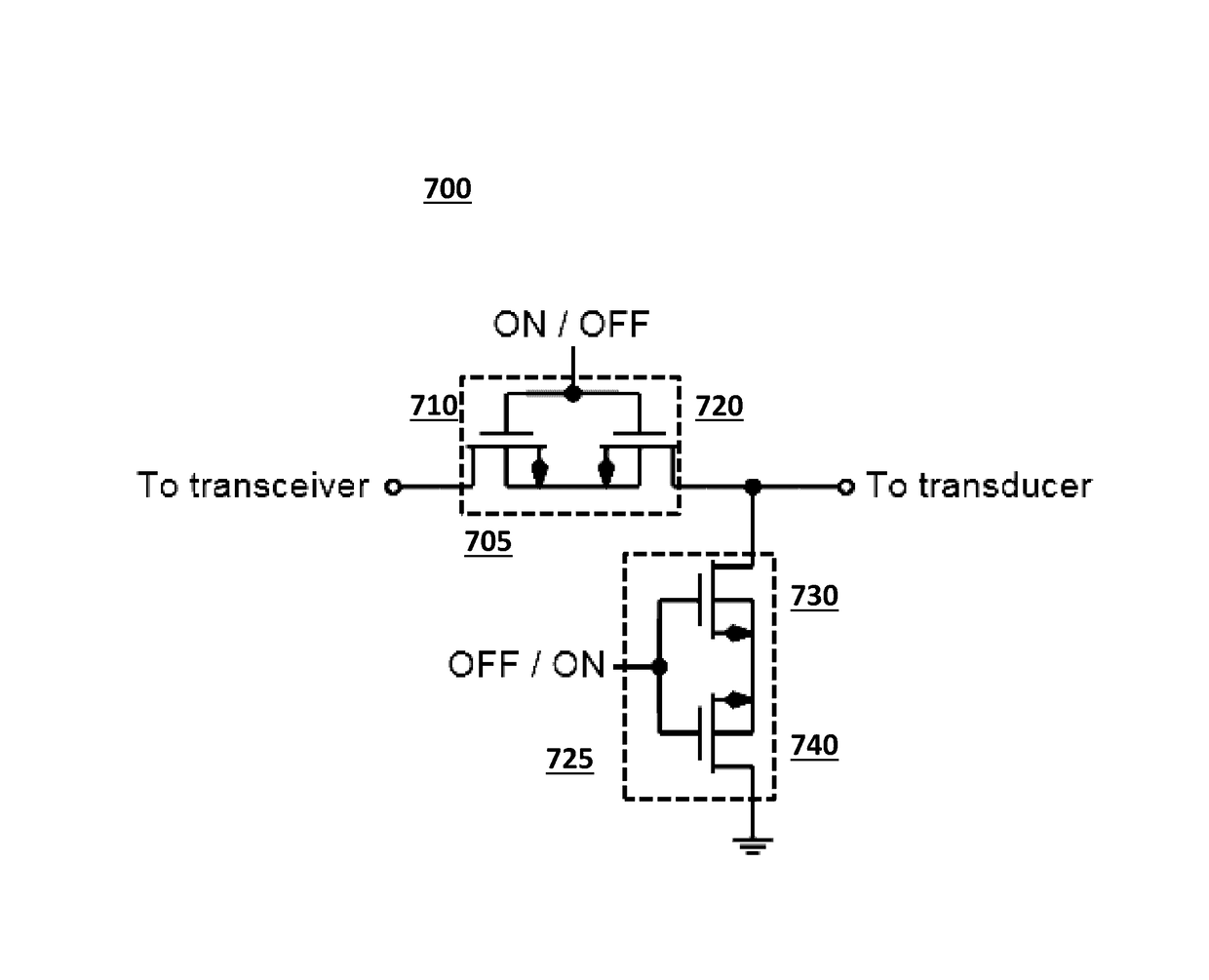
[0023]FIG. 7 depicts an embodiment of the invention. Analog switch 700 is a modified version of T-switch 600 where one of the series butterfly transistor pairs has been removed. Analog switch 700 comprises butterfly transistor pair 705 (comprising NMOS transistors 710 and 720) and shunt butterfly transistor pair 725 (comprising NMOS transistors 730 and 740), which performs a shunting function. NMOS transistors 710, 720, 730, and 740 each comprise a thin gate oxide layer. A thin gate oxide layer typically ranges between 100-200 angstrom. In this configuration, butterfly transistor pair 705 can be considered to be a conducting means for connecting a high voltage source to a transceiver, and shunt butterfly transistor pair 725 can be considered to be a shunting means for shunting current from a terminal of the conducting means to ground.

[0024]The on-resistance of analog switch 700 is approximately half of the on-resistance of prior art T-switch 600, and the parasitic capacitance of ana...


PUM


Abstract

An improved analog switch for use in an ultrasound elastography probe is disclosed. The improved analog switch results in less heat dissipation compared to prior art analog switches.

Description

PRIORITY CLAIM[0001]This application claims priority to Chinese Patent Application No. 201510644537.6, filed on Oct. 8, 2015, and titled “An Optimized CMOS Analog Switch” (in Mandarin), which is incorporated herein by reference.FIELD OF THE INVENTION[0002]An improved analog switch for use in an ultrasound elastography device is disclosed. The improved analog switch results in less heat dissipation compared to prior art analog switches.BACKGROUND OF THE INVENTION[0003]Recent developments in ultrasound imaging systems include the use of shear wave elastography. FIG. 1 depicts prior art ultrasound elastography device 100, which comprises transducer 105. Transducer 105 uses acoustic radiation force to induce a “push” pulse 150 into soft tissue 110 that results in shear waves 140. Soft tissue 110 comprises stiff lesion 120 (which could be a tumor or other medical abnormality), which includes or is near region of interest 130. The tissue's stiffness is computed based upon how fast the res...

Claims


Application Information

Patent Timeline
Patent Type & Authority Applications(United States)
IPC IPC(8): H03K17/16A61B8/00A61B8/08
CPCH03K17/161A61B8/4483A61B8/485A61B8/469A61B8/546H03K17/6874H03K17/693H03K2217/0054H04B1/48
Inventor KO, ISAACHO, KA WAICHAN, WAN TIM
Owner MICROCHIP TECH INC
Why Eureka
Try Eureka