

Indium phosphide smoothing and chemical mechanical planarization processes
a technology of indium phosphide and chemical mechanical planarization, which is applied in the direction of basic electric elements, polishing compositions with abrasives, electric apparatus, etc., can solve problems such as deformation densities, and achieve the effect of suppressing the generation of phosphine gas
- Summary
- Abstract
- Description
- Claims
- Application Information
AI Technical Summary
Benefits of technology
Problems solved by technology
Method used
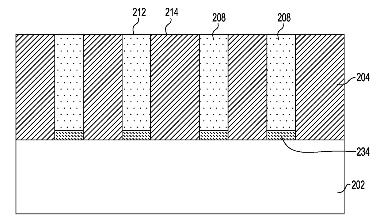
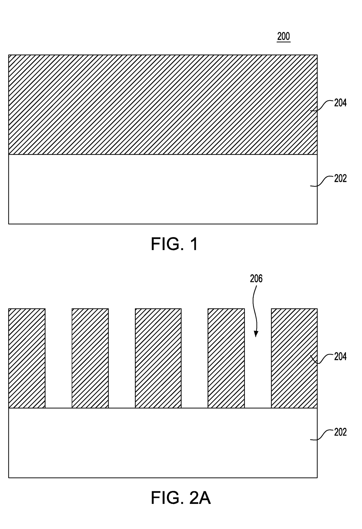
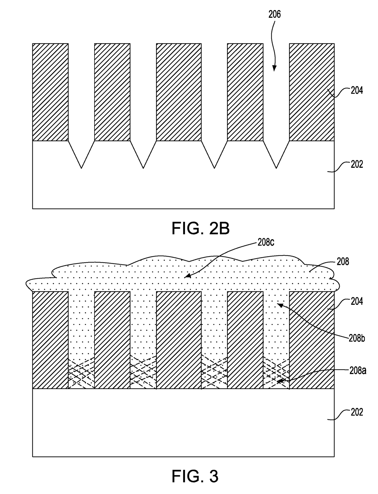
Image

Examples
example 1
[0085]The second slurry composition having a pH within a range of 3 to 5 was prepared and included:[0086]a) abrasive particle such as, 2% by weight of colloidal silica abrasive dispersed in water;[0087]b) an acidic pH modulator, such as, for instance, phosphoric acid within a range of 0.0004 to 0.0006% by weight; and[0088]c) an oxidizer, such as, for instance, 30% solution of hydrogen peroxide from 10 to 100 mL, and more preferably, 25 mL / L.
example 2
[0089]The second slurry composition having a pH within a range of 3 to 5 was prepared and included:[0090]a) abrasive particle such as, 1% by weight of colloidal silica abrasive dispersed in water;[0091]b) an acidic pH modulator, such as, for instance, phosphoric acid within a range of 0.0004 to 0.0006% by weight; and[0092]c) an oxidizer, such as, for instance, 30% solution of hydrogen peroxide of 50 mL / L.
example 3
[0093]The second slurry composition having a pH within a range of 3 to 6 was prepared and included:[0094]a) abrasive particle such as, 1% by weight of colloidal silica abrasive dispersed in water;[0095]b) an acidic pH modulator, such as, for instance, phosphoric acid within a range of 0.0004 to 0.0006% by weight; and[0096]c) an oxidizer, such as, for instance, 30% solution of hydrogen peroxide within a range of 10 to 100 mL / L, and more preferably, 50 mL / L; and[0097]d) soluble polyelectrolyte such as, for instance, polystyrene sulfonate (having a molecular weight of 10,000 to 400,000) within a range of 0.01 to 0.1 percent by weight, and more preferably, 0.002 to 0.003 percent by weight.
PUM
| Property | Measurement | Unit |
|---|---|---|
| roughness | aaaaa | aaaaa |
| thickness | aaaaa | aaaaa |
| thickness | aaaaa | aaaaa |
Abstract
Description
Claims
Application Information