Method of electroplating copper into a via on a substrate from an acid copper electroplating bath
- Summary
- Abstract
- Description
- Claims
- Application Information
AI Technical Summary
Benefits of technology
Problems solved by technology
Method used
Image

Examples
example 1
[0044]Copper electroplating baths were prepared by first combining 60 g / L Cu2+ from CuSO4.5H2O, 60 g / L H2SO4, and 50 mg / L Cl− from 1N HCl, and then adding 6 mg / L of the accelerator sodium bis(sulfopropyl)disulfide from stock solution, 17.5 mg / L of a leveler which was a reaction product of butyl diglycidyl ether, 75% 4-phenyl imidazole and 25% imidazole from a stock solution. Each bath included Suppressors 1 and 2 in amounts shown in Table 1 below.
TABLE 1Suppres-sor NoSuppressor MaterialAmountTrade Name1R—O—(PO)m—(EO)n—H120ECOSURF ™diblock copolymermg / LEH 14Mw = 1037 g / molesurfactant2HO—(EO)a—(PO)b—(EO)aH100PLURONIC ™triblock copolymer,mg / LP84Mw = 4200 g / molesurfactant
R is a branched 2-ethylhexane moiety. The HLB of the triblock copolymer was determined to be 19 using the Davies method. Variables used for calculating the HLB by the Davies method are in the table below:
TABLE 2Mw#EO#PO#CH# Ether#OH% EOEOMw POGroupsGroupsGroupsGroupsGroups40168025203843205812
example 2
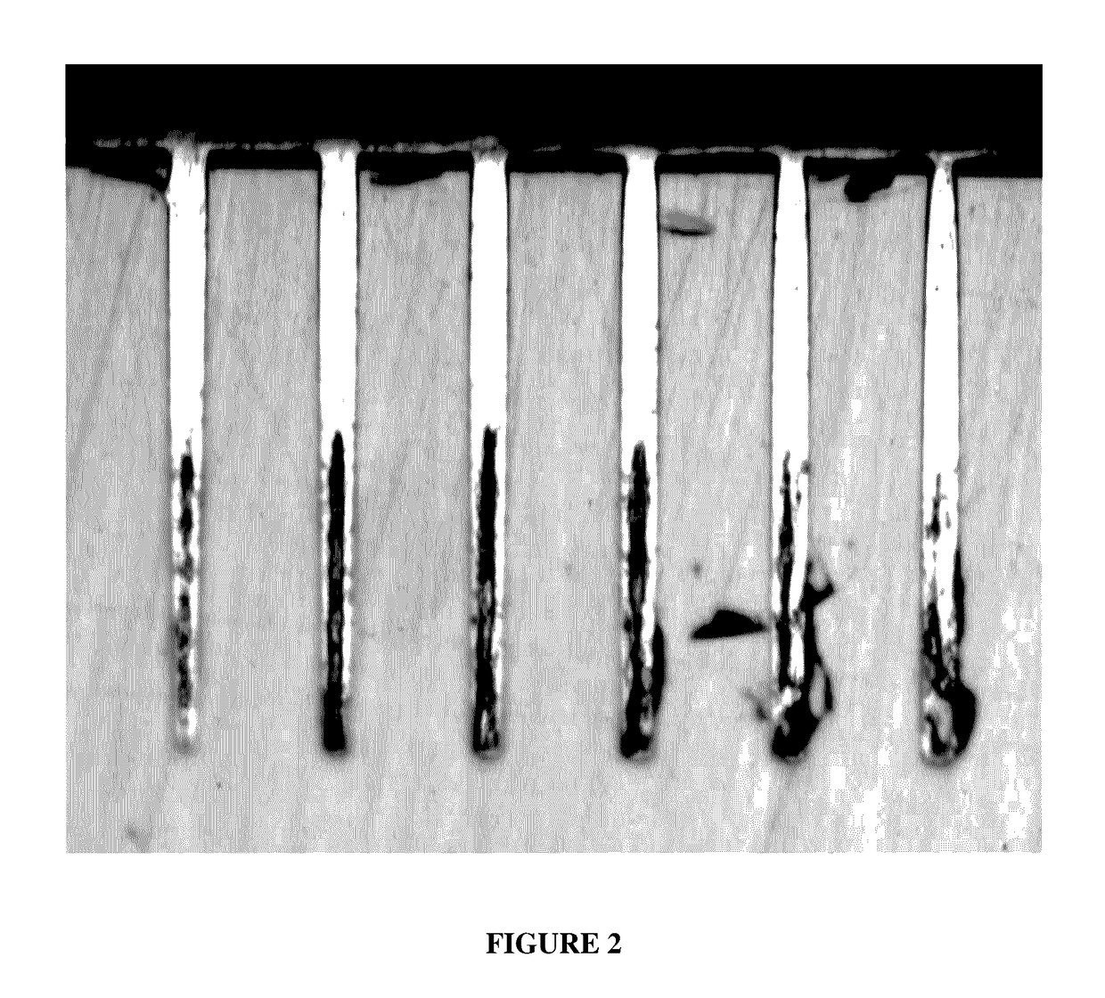
[0045]Via fill testing was performed on various test wafer coupons having 5 μm diameter×55 μm deep TSVs. The coupons were attached to the plating head of a segment plater with conductive copper tape, which was then covered by platers tape from 3M, Minneapolis, Minn. All coupons were subjected to a 5 minute deionized water spray prior to plating. Each wafer coupon acted as the cathode and was rotated by a Pine Instruments MSRX rotator at 50 rpm and was contacted with the electroplating baths from Example 1. The temperature of the electroplating bath was 25° C. The plating waveform used to monitor surface (swirl) defects is reported in Table 3, where CD is the current density. The dynamic surface tension of each of the plating baths was measured at 25° C. using a Krüss BP100 bubble pressure tensiometer at a surface age of 30 seconds and was determined to be 36.7 mN / m.
TABLE 3Cu Deposit thickness, ÅCD, mA / cm2Time, min.Hot entry00.10Step 1150016.76Step 2200024.50Step 3250033.75Step 44000...
example 3
[0047]The method disclosed in Example 2 was repeated except that the suppressor combination had the components in Table 4.
TABLE 4Suppres-sor NoSuppressor MaterialAmountTrade Name1R—O—(PO)m—(EO)n—H120ECOSURF ™diblock copolymermg / LEH 14Mw = 1037 g / molesurfactant2HO—(EO)a—(PO)b—(EO)a—OH100PLURONIC ™triblock triblock copolymer,mg / LP85Mw = 4600 g / molesurfactant
R is as defined in Example 1 above. The HLB for the triblock copolymer was determined to be 24 using the Davies method. Variables used for calculating the HLB are in the table below:
TABLE 5Mw#EO#PO#CH# Ether#OH% EOEOMw POGroupsGroupsGroupsGroupsGroups50230023005240224922
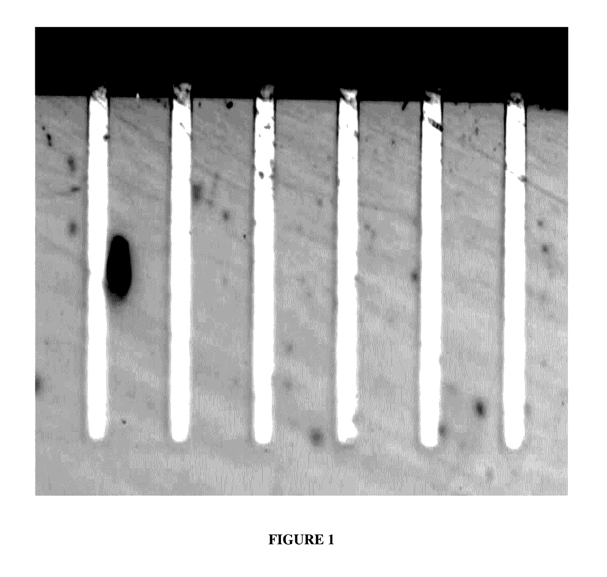
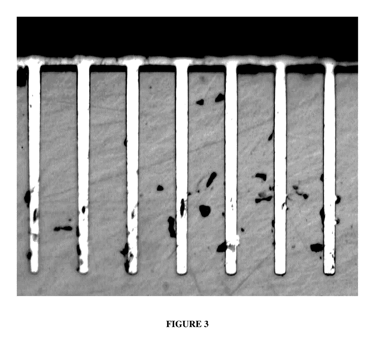
[0048]After the TSVs were filled they were analyzed by the same method described in Example 2. No voids were observed in the samples. The cross-sections of the samples appeared substantially the same as shown in FIG. 1. All the samples had bright copper surfaces. There were no observable defects on the copper deposits.
PUM
| Property | Measurement | Unit |
|---|---|---|
| Molar mass | aaaaa | aaaaa |
| Molar mass | aaaaa | aaaaa |
| Surface energy | aaaaa | aaaaa |
Abstract
Description
Claims
Application Information
PatSnap Eureka turns technology decisions into work you can execute. Powered by our Innovation Knowledge Graph, it runs expert workflows across engineering, life sciences, materials and intellectual property. Get your review-ready output in minutes.


