Novel terminations

a technology of electronic support structure and termination, which is applied in the direction of semiconductor devices, semiconductor/solid-state device details, electrical apparatus, etc., can solve the problems of generating solder bumps on the substrate in ever tighter pitches, more and more accurate and more expensive, and certain susceptibility of disconnected contacts and electrical open failures, etc., to achieve tighter pitch, lower cost, and high yield

Active Publication Date: 2017-04-27
ZHUHAI ADVANCED CHIP CARRIERS & ELECTRONICS SUBSTRATE SOLUTIONS TECH
View PDF0 Cites 0 Cited by
  • Summary
  • Abstract
  • Description
  • Claims
  • Application Information

AI Technical Summary

Benefits of technology

The present invention introduces new termination designs that facilitate the creation of more cost-effective, reliable, and compact interposers and multilayer support structures with tighter pitch. Additionally, the invention provides a method for directly attaching an IC chip to an electronic support structure using flip chip technology, resulting in strong anchoring.

Problems solved by technology

Generating solder bumps on the substrate in ever tighter pitches is tricky in that the current methods of stencil printing, solder ball drops or solder bump electro plating are required to be more and more accurate and more expensive in order to overcome the risk of shorting between nearby connections at the finer pitches.
This leads to a certain susceptibility of disconnected contacts and electrical open failures.
This solution is somewhat more expensive than other termination technologies because of the additional processing and the different compositions of solderable materials that are required.
Nevertheless, due to the relatively large thickness of copper pillars as compared to the conductor layer and since each of the copper pillars must be accurately aligned on an underlying conductor layer, such pillars are subject to separation spacing limitations that can adversely affect their application in tight pitch flip chip devices.
Furthermore, it will be appreciated that an additional copper pillar layer increases the number of process steps required for manufacturing such substrates thereby increasing fabrication costs and lowering yields.

Method used


Image

  • Novel terminations
  • Novel terminations
  • Novel terminations

Examples


Embodiment Construction

[0040]In the description hereinbelow, support structures consisting of metal vias in a dielectric matrix, particularly, copper via posts in a polymer matrix, such as polyimide or epoxy or BT (Bismaleimi de / Triazine) or their blends. Such dielectrics may be reinforced with glass fibers and applied as prepregs. Other embodiments use other thermoplastic or thermoset polymers.

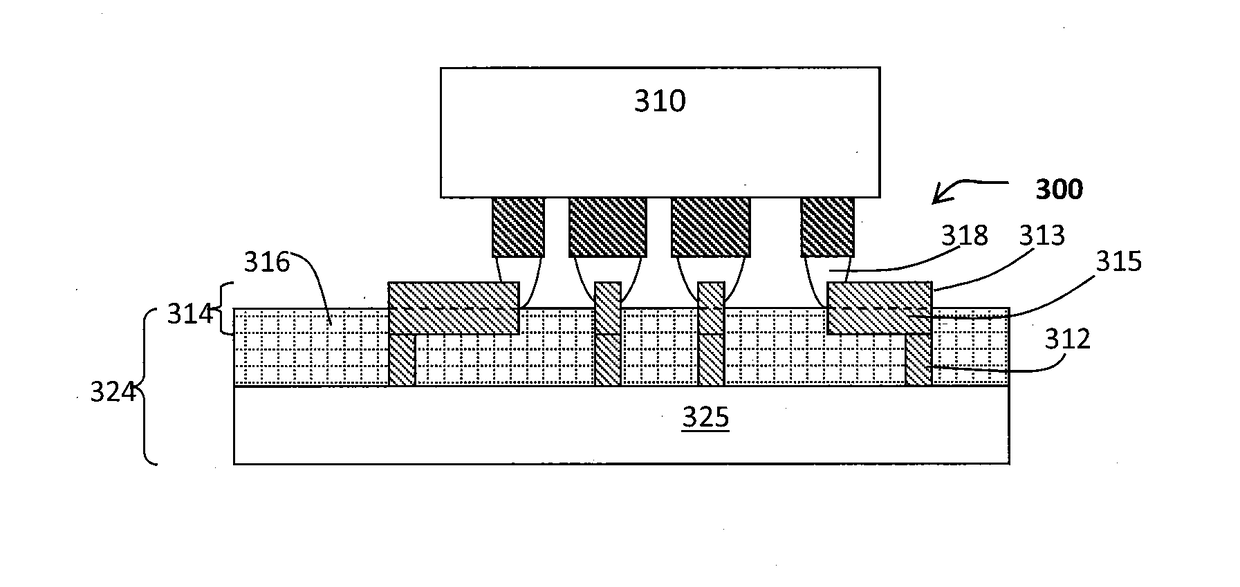
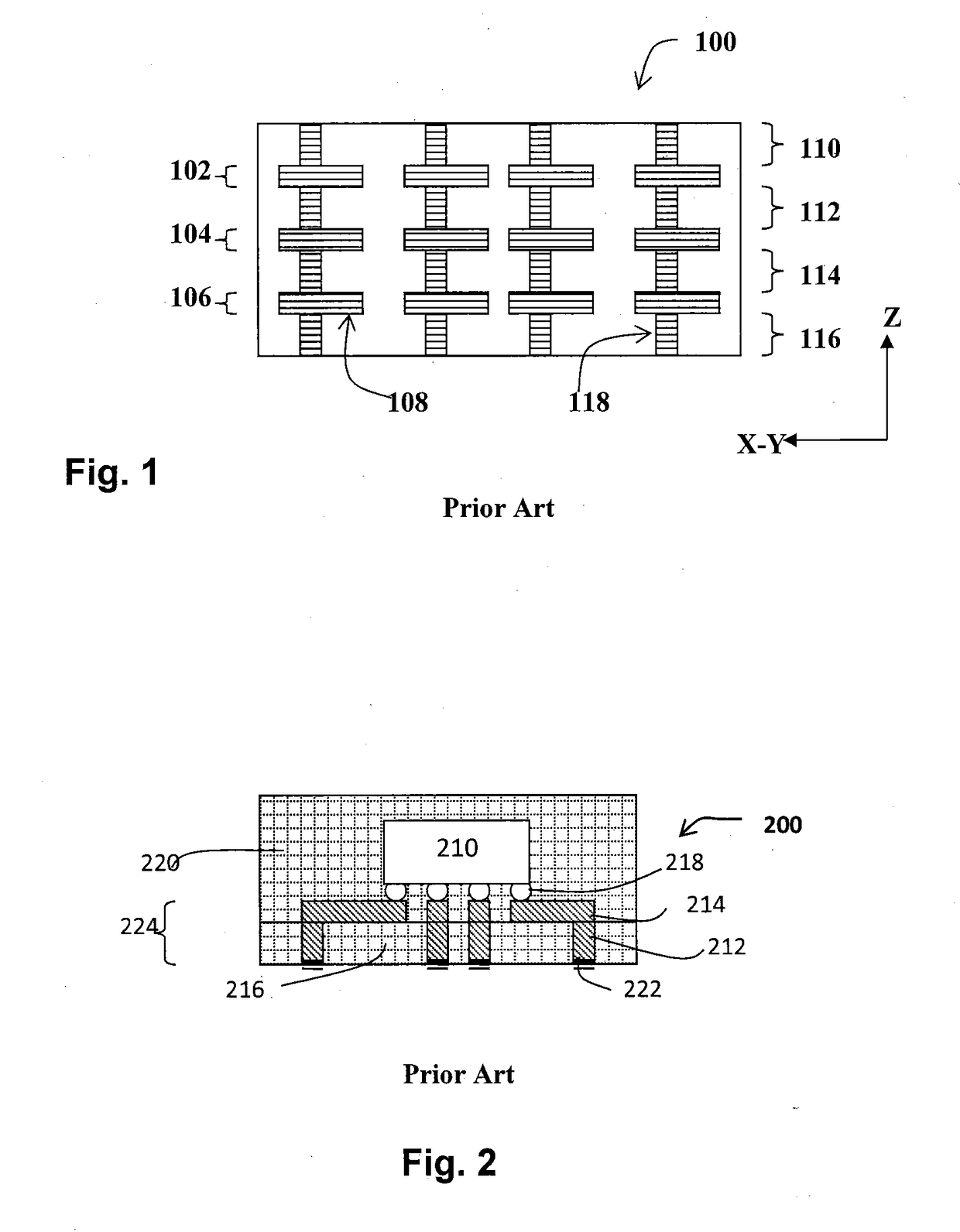
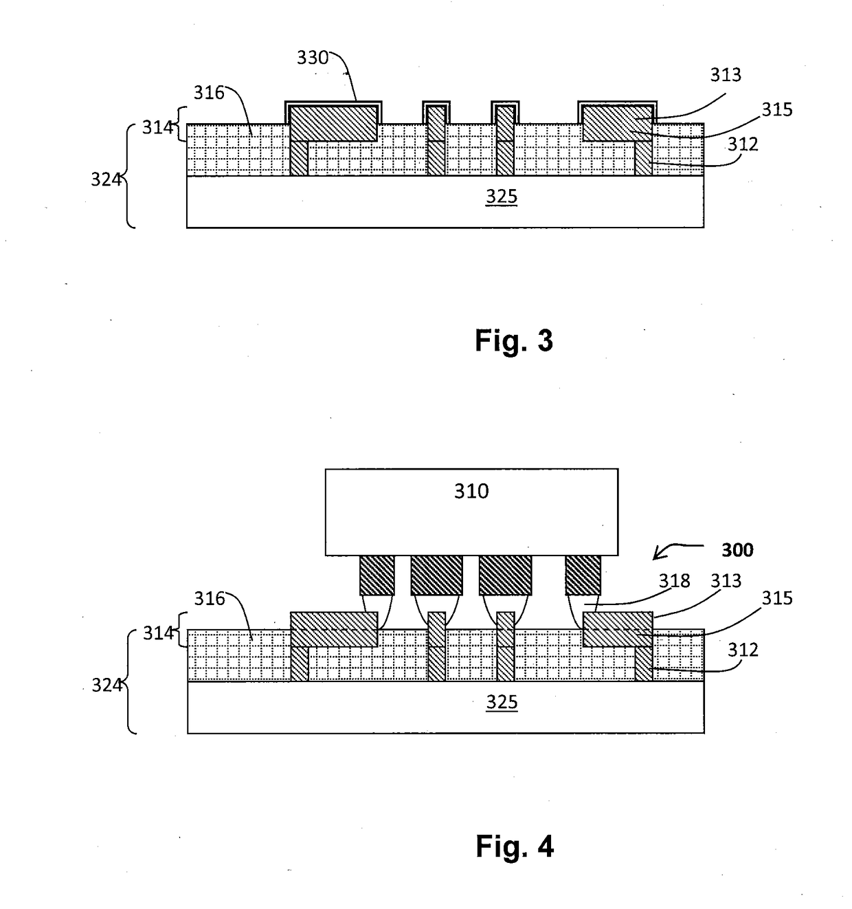
[0041]FIG. 1 is a simplified section through a multilayer composite support structure of the prior art. As described in U.S. Pat. No. 7,682,972, U.S. Pat. No. 7,669,320 and U.S. Pat. No. 7,635,641, for example, multilayer support structures 100 of the prior art include functional layers 102, 104, 106 of components or features 108 separated by layers of dielectric 110, 112, 114, 116, which insulate the individual layers. Vias 118 through the dielectric layer provide electrical connection between features 108 in the adjacent functional or feature layers 102, 104, 106. Thus the feature layers 102, 104, 106 include fea...


PUM

PropertyMeasurementUnit
depthaaaaaaaaaa
roughnessaaaaaaaaaa
thickaaaaaaaaaa

Abstract

An electronic support structure comprising one or more layers of copper features such as copper routing layers, laminated within a dielectric material comprising continuous glass fibers in a polymer matrix wherein pairs of adjacent layers of copper features are coupled by a via layer, and where terminations on at least one side of the electronic support structure comprise a modified bond-on-trace attachment sites comprising selectively exposed top and partial side surfaces of copper features in an outer layer of copper features for conductive coupling solder.

Description

BACKGROUND[0001]Field of the Invention[0002]The present invention relates to terminations for multilayer electronic support structures such as interposers, and to methods of manufacturing of same.[0003]Description of the Related Art[0004]Driven by an ever greater demand for miniaturization of ever more complex electronic components, consumer electronics such as computing and telecommunication devices are becoming more integrated. This has created a need for support structures such as IC substrates and IC interposers that have a high density of multiple conductive layers and vias that are electrically insulated from each other by a dielectric material.[0005]The general requirement for such support structures is reliability and appropriate electrical performance, thinness, stiffness, planarity, good heat dissipation and a competitive unit price.[0006]Among the high density leading technologies used to interconnect the Substrate to Chips is the well-established “Flip Chip” technology, ...

Claims


Application Information

Patent Timeline
Patent Type & Authority Applications(United States)
IPC IPC(8): H01L21/48H01L23/498
CPCH01L21/4853H01L21/4857H01L2021/60022H01L23/49822H01L23/49838H01L23/49827H01L21/486H01L24/13H01L24/16H01L24/81H01L2224/0401H01L2224/13023H01L2224/131H01L2224/16013H01L2224/16238H01L2224/81191H01L2224/81395H01L2924/381H01L2924/00014H01L2924/014
Inventor HURWITZ, DRORHUANG, ALEX
Owner ZHUHAI ADVANCED CHIP CARRIERS & ELECTRONICS SUBSTRATE SOLUTIONS TECH
Why Eureka
Try Eureka