Semiconductor laser device

a laser device and semiconductor technology, applied in semiconductor lasers, lasers, electrical equipment, etc., can solve the problems of limited improvement of power conversion efficiency during high output power, and achieve the effect of improving power conversion efficiency and high output power

Active Publication Date: 2017-04-27
MITSUBISHI ELECTRIC CORP
View PDF1 Cites 2 Cited by
  • Summary
  • Abstract
  • Description
  • Claims
  • Application Information

AI Technical Summary

Benefits of technology

[0007]The present invention has been implemented to solve the above-described problems and it is an object of the presen...

Problems solved by technology

The semiconductor laser device having a conventional asymmetric structure can achieve both a reduction of the threshold curr...

Method used


Image

  • Semiconductor laser device
  • Semiconductor laser device
  • Semiconductor laser device

Examples


first embodiment

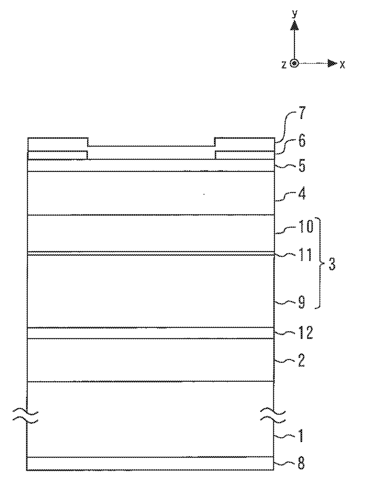
[0041]FIG. 1 is a cross-sectional view illustrating a semiconductor laser device according to a first embodiment of the present invention. An n-type AlGaAs cladding layer 2 having an Al composition ratio of 0.250 and a layer thickness of 1.5 μm is formed on an n-type GaAs substrate 1. A light guide layer 3 is formed on the n-type AlGaAs cladding layer 2.

[0042]A p-type AlGaAs cladding layer 4 having an Al composition ratio of 0.250 and a layer thickness of 1.5 μm is formed on the light guide layer 3. A p-type GaAs contact layer 5 having a layer thickness of 0.2 μm is formed on the p-type AlGaAs cladding layer 4.

[0043]A SiN film 6 having a film thickness of 0.2 μm is formed on the p-type GaAs contact layer 5. A p-type electrode 7 is formed on the SiN film 6 and electrically connected to the p-type GaAs contact layer 5 through an opening of the SiN film 6. An n-type electrode 8 is formed on a rear surface of the n-type GaAs substrate 1.

[0044]The light guide layer 3 includes an n-side A...

second embodiment

[0058]FIG. 8 is a cross-sectional view illustrating a semiconductor laser device according to a second embodiment of the present invention. The light guide layer 3 of the present embodiment includes a first light guide layer 13 formed on the n-type AlGaAs cladding layer 2, and second light guide layers 14 and 15 formed on the first light guide layer 13. The active layer 11 is formed between the second light guide layers 14 and 15. The first light guide layer 13 is AlGaAs having an Al composition ratio of 0.210. The second light guide layers 14 and 15 are AlGaAs having the same Al composition ratio of 0.190. The sum of a layer thickness dn2 of the second light guide layer 14 and a layer thickness dp of the second light guide layer 15 is 450 nm and is smaller than a layer thickness 750 nm of the first light guide layer 13.

[0059]The sum of layer thicknesses of the first light guide layer 13 and the second light guide layers 14 and 15 is 1200 nm. Note that the refractive index of AlGaAs...

third embodiment

[0062]FIG. 11 is a cross-sectional view illustrating a semiconductor laser device according to a third embodiment of the present invention. A p-type AlGaAs low-refractive-index layer 16 having an Al composition ratio of 0.600 and a layer thickness of 40 nm is formed between the light guide layer 3 and the p-type AlGaAs cladding layer 4. The rest of the configuration is similar to that of the first embodiment.

[0063]FIG. 12 is a diagram illustrating a refractive index distribution along a crystal growing direction in the vicinity of the active layer of the semiconductor laser device according to the third embodiment of the present invention. The p-type AlGaAs low-refractive-index layer 16 has a lower refractive index nl2 than the refractive index nc of the p-type AlGaAs cladding layer 4. Note that the refractive index of AlGaAs having an Al composition ratio of 0.600 with respect to light having a wavelength of 915 nm is 3.1846.

[0064]As described in the first embodiment, the insertion...


PUM


Abstract

An active layer is provided on a side closer to the second conductivity type cladding layer than a center of the light guide layer in the light guide layer. A first conductivity type low-refractive-index layer is formed between the first conductivity type cladding layer and the light guide layer and has a refractive index which is lower than a refractive index of the first conductivity type cladding layer. A layer thickness d of the light guide layer is a value at which a high-order mode equal to or higher than a first-order mode is permissible in a crystal growing direction by satisfying
2πλng2-nc2d2π2.
The active layer is disposed at a position where a light confinement of the active layer becomes smaller compared to a case in which the active layer is disposed at a center of the light guide layer while there is not the first conductivity type low-refractive-index layer.

Description

BACKGROUND OF THE INVENTIONField[0001]The present invention relates to a semiconductor laser device capable of improving power conversion efficiency during high output power.Background[0002]As a light guide layer structure of a semiconductor laser device, there are structures such as an asymmetric structure in which a peak position of light confinement is displaced from a center of the light guide layer to a p-type cladding layer side and a symmetric structure in which an active layer is located at a center of the light guide layer and a peak position of light confinement is also located at the center of the light guide layer. A semiconductor laser is proposed in which an active layer is disposed at a position where light confinement of the active layer increases in the asymmetric structure than that in the symmetric structure (e.g., see Patent Literature 1: JP 2014-197598 A and Patent Literature 2: JP 2015-23180 A). This makes it possible to achieve both a reduction of a threshold ...

Claims


Application Information

Patent Timeline
IPC IPC(8): H01S5/20H01S5/22
CPCH01S5/22H01S5/2031H01S5/2004H01S5/3213H01S5/34313
Inventor SHIGIHARA, KIMIO
Owner MITSUBISHI ELECTRIC CORP
Why Eureka
Try Eureka