Method of manufacturing semiconductor device

a manufacturing method and semiconductor technology, applied in the direction of semiconductor devices, basic electric elements, electrical appliances, etc., can solve the problems of increasing processing time, material requirements that cannot be met, and problem with low-temperature process, so as to prevent a reduction in yield, increase the frequency of maintenance, and increase the effect of productivity

Active Publication Date: 2017-06-08
MITSUBISHI ELECTRIC CORP
View PDF4 Cites 4 Cited by
  • Summary
  • Abstract
  • Description
  • Claims
  • Application Information

AI Technical Summary

Benefits of technology

[0009]In view of the above-described problem, an object of the present invention is to provide a method of manufacturing a semiconductor device capable of preventing a reduction in yield and an increase in frequency of maintenance and increasing the productivity while using the conventional apparatus without being specially modified.
[0011]In the present invention, the SiC substrate, which is a material difficult to etch, is dry-etched by using the resist as a mask instead of using a metal mask which becomes a cause of falls of debris by attaching to a ceiling plate without evaporating at the time of etching. A reduction in yield and an increase in frequency of maintenance caused by falls of debris can thereby be prevented. Since the resist is applied on the resist separation layer, even the resist difficult to separate and dissolve in an ordinary situation can be separated from the SiC substrate 1 by removing the resist separation layer. Dry etching can therefore be performed at a high temperature of 200° C. or higher by using as a mask the resist capable of retaining a shape at a temperature of 200° C. or higher. The processing rate is improved thereby, thus improving the productivity. Also, a conventional manufacturing apparatus can be used without being specially modified.

Problems solved by technology

However, there are presently no materials satisfying the requirements, such as a resist capable of retaining a shape even at a high temperature of 200° C. or higher and capable of being easily separated or dissolved and a wax (adhesive) not dissolved at a temperature of 150° C. or higher.
Therefore the problem with a low-temperature process cannot be avoided.
This means that the processing time is increased due to a low processing rate, and that a metal mask is eventually used since any resist cannot endure processing for a long time period.
The metal mask generates a large amount of contamination, causes falls of debris from a ceiling plate onto the wafer and chamber walls, and causes a reduction in productivity, a reduction in yield and an increase in frequency of maintenance.
Each of the above-described methods, however, requires extensively modifying the conventional apparatus and is incapable of radically inhibiting generation of nonvolatile products which cause falls of debris.

Method used


Image

  • Method of manufacturing semiconductor device
  • Method of manufacturing semiconductor device
  • Method of manufacturing semiconductor device

Examples


first embodiment

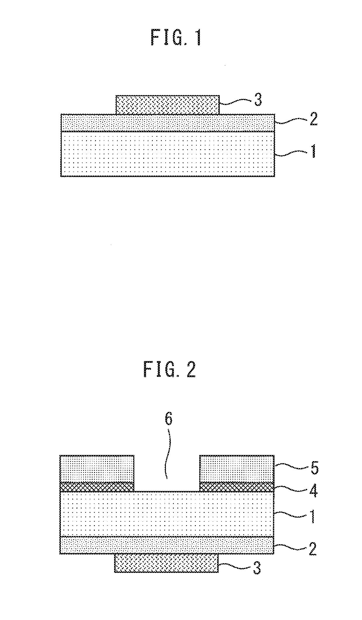
[0016]FIGS. 1 to 5 are sectional views showing a method of manufacturing a semiconductor device according to a first embodiment of the present invention. First, as shown in FIG. 1, a GaN-on-SiC substrate is formed by epitaxially growing a GaN epi-layer 2 on a front surface of an SiC substrate 1. A source electrode 3 is formed on the GaN epi-layer 2.

[0017]Subsequently, as shown in FIG. 2, a resist separation layer 4, which is not cured and soluble in a chemical solution even at a high temperature of 400° C., is applied to a back surface of the SiC substrate 1. The material of the resist separation layer 4 is, for example, Omnicoat, which is an aliphatic polyimide-based resist developed as the material of a sacrificial layer for a permanent resist.

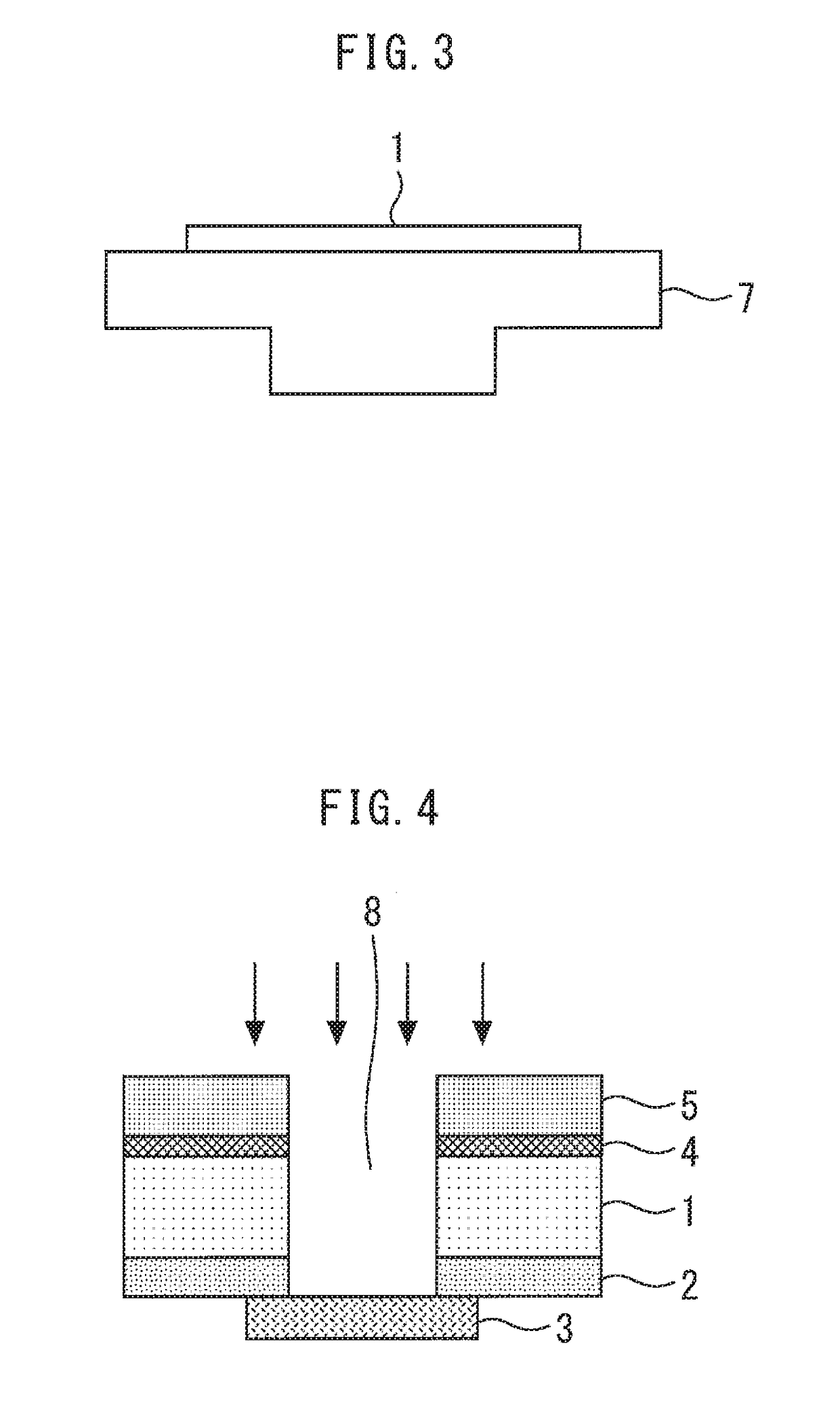
[0018]Subsequently, a resist 5 having high dry resist resistance and capable of retaining a shape in a temperature range from 200° C. to about 400° C. and having a thickness (ordinarily 100 μm to 200 μm) equal to or larger than a work substr...

second embodiment

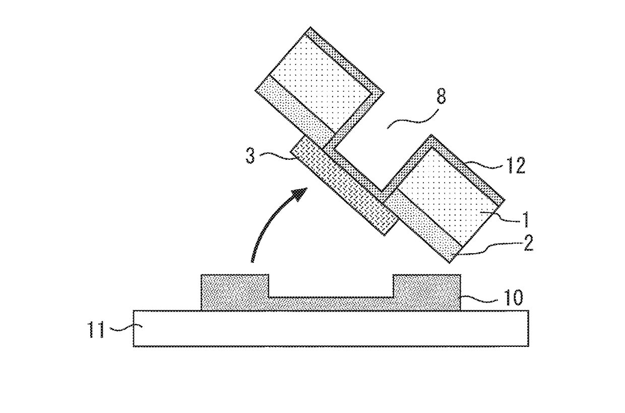
[0025]FIGS. 6 to 8 are sectional views showing a method of manufacturing a semiconductor device according to a second embodiment of the present invention. The present embodiment corresponds to a more practical mode of processing for forming a via hole in GaN-on-SiC by using a support substrate in the first embodiment.

[0026]As shown in FIG. 6, a substrate separation layer 9 is formed on the front surface side of the SiC substrate 1 on which the GaN epi-layer 2 and the source electrode 3 are formed. It is desirable to use, as the substrate separation layer 9, Omnicoat, which is an aliphatic polyimide-based resist, in order to protect the GaN epi-layer 2 and the source electrode 3 on the front surface side.

[0027]Subsequently, an adhesive 10 is applied on the substrate separation layer 9. The adhesive 10 is cured by hard baking at a temperature of 200° C. or higher, e.g., about 300° C., thereby bonding the SiC substrate Ito a support substrate 11. The adhesive 10 is a liquid material wh...


PUM

PropertyMeasurementUnit
temperatureaaaaaaaaaa

Abstract

A method of manufacturing a semiconductor device includes: forming a resist separation layer on a first main surface of a SiC substrate; applying a resist retaining a shape at a temperature of 200° C. or higher on the resist separation layer; patterning the resist by photolithography; heating a stage an which the SiC substrate is placed to a temperature of 200° C. or higher by a temperature control function, and dry-etching the SiC substrate by using the patterned resist as a mask to form a via hole; and after forming the via hole, removing the resist separation layer to separate the resist from the SiC substrate.

Description

BACKGROUND OF THE INVENTION[0001]Field[0002]The present invention relates to a method of manufacturing a semiconductor device.[0003]Background[0004]To secure a certain radiofrequency characteristic of a compound semiconductor device, a so-called via hole structure which provides a conduction path from a back surface of a substrate to a source electrode on a front surface of the substrate is formed by dry etching. This via hole forming is performed ordinarily by attaching a work substrate on a support substrate with an adhesive easily soluble in a chemical solution and capable of attachment and separation even at a temperature of about 150° C. In the case of GaN-on-SiC, rather than a resist mask, a metal mask more difficult to etch than SiC is ordinarily used because of the difficult-to-etch characteristic of the SiC substrate for example, IEEE TRANSACTIONS ON PLASMA SCIENCE, VOL. 32, No. 3, JUNE 2004).[0005]In a case where a via hole is formed in a compound semiconductor device, suc...

Claims


Application Information

Patent Timeline
Patent Type & Authority Applications(United States)
IPC IPC(8): H01L21/768H01L21/027H01L21/683H01L21/04
CPCH01L21/76898H01L21/0475H01L2221/68381H01L21/6836H01L2221/68372H01L21/0274H01L21/0273H01L21/3081H01L21/31133H01L21/6835H01L29/2003H01L29/4175
Inventor MIKI, KOHEIONOE, KAZUYUKIMIYAKUNI, SHINICHI
Owner MITSUBISHI ELECTRIC CORP
Why Eureka
Try Eureka