LED illumination apparatus and manufacturing method thereof

a technology of light-emitting diodes and illumination apparatuses, which is applied in the direction of lighting and heating apparatus, semiconductor devices for light sources, planar light sources, etc., can solve the problems of low reliability for mass production, failure to meet the requirements of high-power heat dissipation and environmental protection, and the illumination range is not provided with any solution, etc., to achieve the effect of improving heat dissipation efficiency, less material, and illumination rang

Inactive Publication Date: 2017-06-29
LONGWIDE TECH
View PDF0 Cites 6 Cited by
  • Summary
  • Abstract
  • Description
  • Claims
  • Application Information

AI Technical Summary

Benefits of technology

[0026]Therefore, it is a primary objective of the present invention to overcome the aforementioned problems of the conventional LED illumination apparatus and adopt the concept of combining a 3D light emitting curved surface thermoelectrically, so that the large amount of heat generated by the LED chip can be dissipated by convection through the conductive plate made of a large-area metal.
[0053]4. The conductive plate of the present invention is a thin sheet that consumes less metal material while reducing the weight of the illumination apparatus of the present invention.

Problems solved by technology

TWM337844, a large power LED comprises an electrode pin installed onto a metal plate to increase the heat dissipating area, but such solution does not adopts the structure of a heat transfer contact and has not disclosed a total cooling solution for the illumination apparatus.
Since the specific column-shaped cooling column can just provide illumination in the circumferential direction, such heat dissipation does not provide any solution for the illumination range.
Due to cost, most conventional LED bulbs adopts heat dissipating fins or sheet structures made of aluminum sheet or aluminum die-cast sheet to achieve the effect of environmental friendliness and consume less material.
US2012 / 006215A1, a flexible circuit board is manufactured with several PCB chemical processes, and thus this solution fails to meet the high-power heat dissipation requirement and the environmental protection requirement.
Such process can form the structure more quickly, but it also had disadvantages on the process of cutting the circuit and the follow-up manual process of mounting an LED chip on to the 3D curved surface and the soldering process.
In addition, such solution incurs a high cost and a low reliability for mass production.

Method used


Image

  • LED illumination apparatus and manufacturing method thereof
  • LED illumination apparatus and manufacturing method thereof
  • LED illumination apparatus and manufacturing method thereof

Examples


first embodiment

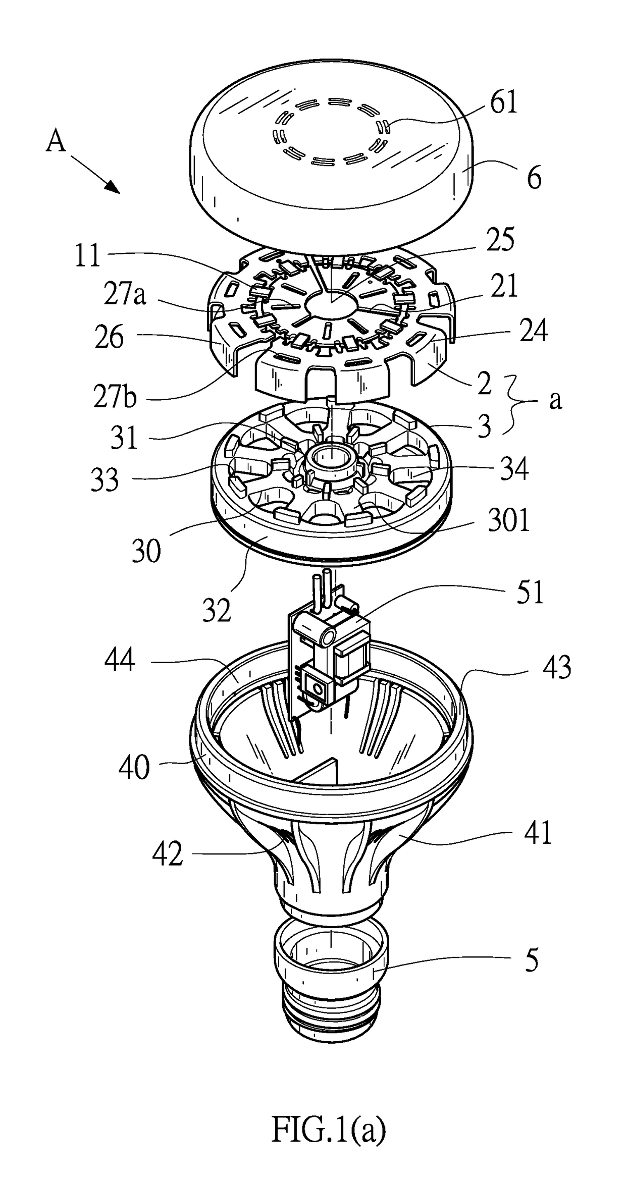
[0112]With reference to FIG. 1(e) for an illumination apparatus of the present invention, the illumination apparatus comprises a conductive plate 2 and a support frame 3 combined with each other; wherein the conductive plate 2 is cut into a plurality of strip structures 20 from a plurality of isolation slots 21 by a stamping board 80, and a plurality of connecting portions 23 is disposed across each isolation slot 21 and combined to form a planar sheet structure (if each electrode slot 22 is disposed at the isolation slot 21, then each auxiliary portion 221 will be disposed across the electrode slot 22 and the isolation slot 21 simultaneously), and each auxiliary portion 221 causes a short circuit which is marked by slant sectional lines for the purpose of recognition.

[0113]With reference to FIG. 1(g) for an illumination apparatus in accordance with an embodiment of the present invention, the illumination apparatus comprises an electrode soldering point protection mechanism of an LE...

fourth embodiment

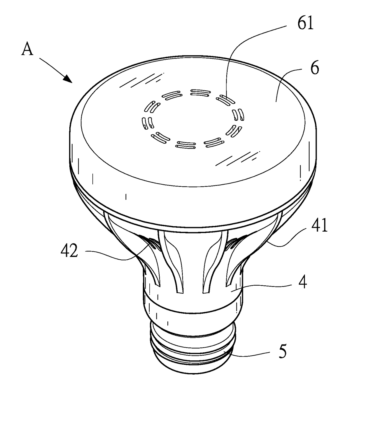
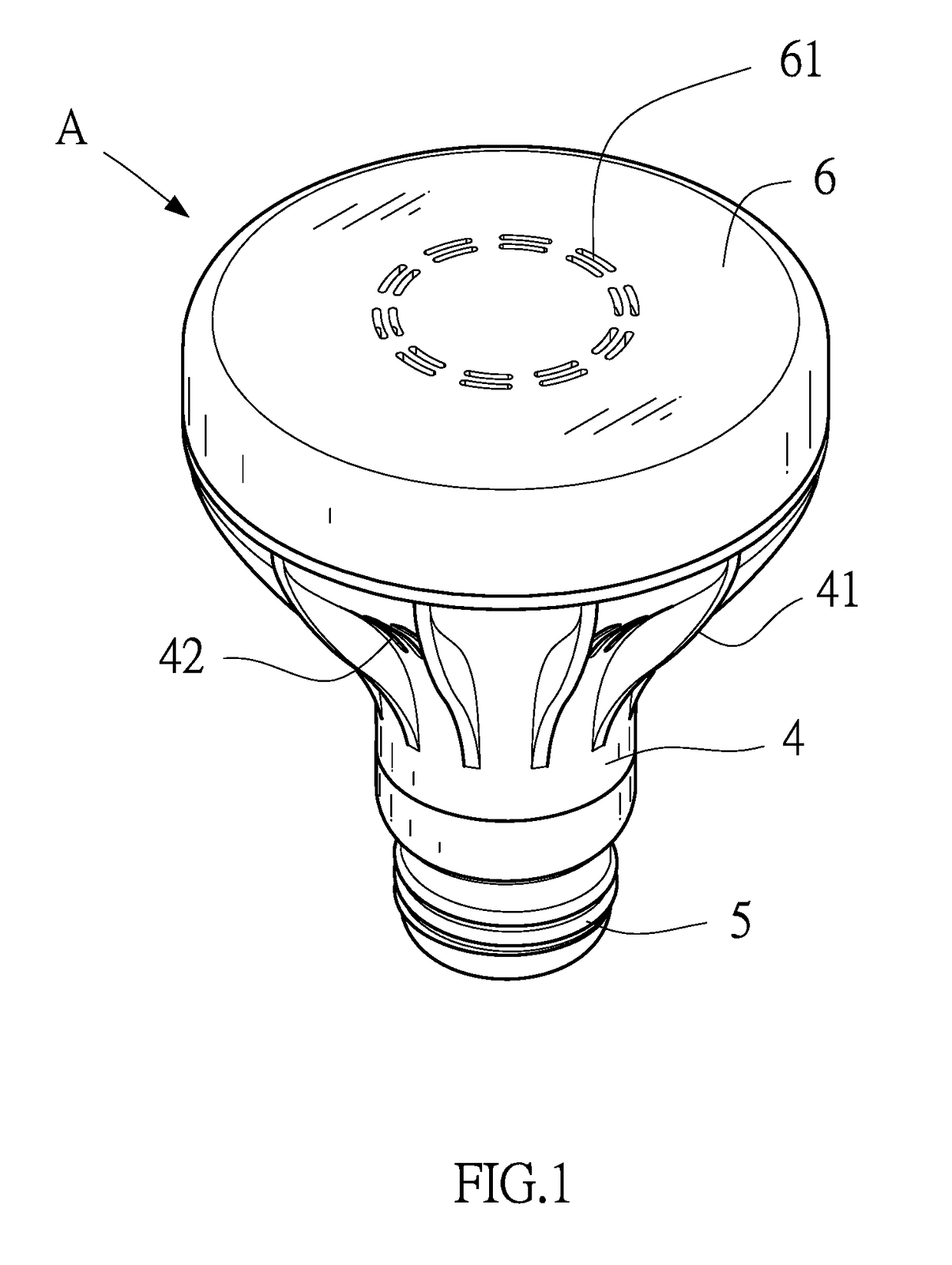
[0164]With reference to FIGS. 4˜4(c) for a hemispherical lamp D of the present invention, an illumination apparatus is comprised of a support frame 3 and a conductive plate 2, and the illumination circuit 10 is comprised of three groups of three-series-three-parallel circuits, and there are a total of 27 LED chips 11. In addition, the illumination apparatus d of the hemispherical lamp comprises a lamp cover 6, a protective cover 7, a conductive plate 2, a plurality of LED chips 11, a support frame 3, and a power module 51.

[0165]When the hemispherical lamp D is installed, the protective cover 7 id disposed at the uppermost position, and the lamp cover 6 is disposed at the lowermost position. Both of the lamp cover 6 and the protective cover 7 are installed into a latch slot 35 of the support frame 3 simultaneously as shown in FIG. 4(b), so as to form the structure of the hemispherical lamp D.

[0166]The lamp cover 6 is a hemispherical opening structure made of a transparent or semi-tra...

second embodiment

[0175]With reference to FIGS. 4, 4(d), and 4(e) for the manufacturing method of the illumination apparatus d of this embodiment, the manufacturing method of this embodiment is substantially the same as that of the aforementioned Referring to FIG. 2(i) as well, the manufacturing method of the illumination apparatus d of this embodiment comprises an unloading process, a mounting process, a reclaiming process, a formation preparation process, a pre-assembling bending process, an assembling process, an auxiliary portion removing process and a post-assembling bending process.

[0176]In the bending process, a stamping mold is provided to press and fix a concentric circular strip fixed planar structure 28 of the spherical curved surface 241 to a predetermined conical angle, and then bending the two bending portions 24c, 24b of the strip structure 20a to form a spherical curved surface 241, so that the circular curved surface 242 forms a conical surface, and the width of the isolation slot 2...


PUM


Abstract

Disclosed are an LED illumination apparatus and its manufacturing method. A metal sheet is stamped to form a conductive plate with 3D space, and the conductive plate includes an illumination circuit, and a support frame for supporting the conductive plate to form different types of illumination apparatuses. The support frame is provided for supporting and fixing the conductive plate to facilitate the conductive plate to form a 3D curved surface, and an LED chip soldering point protection mechanism is provided for protecting each LED chip soldering point, so that the illumination apparatus is applicable for mass production to improve the yield rate and meet the high heat dissipation efficiency, large-range illumination, material saving, lightweight and / or environmental protection requirements.

Description

FIELD OF THE INVENTION[0001]The present invention relates to a light emitting diode (LED) illumination apparatus, and more particularly to the technical field of forming an illumination circuit structure by a stamping technology.BACKGROUND OF THE INVENTION[0002]LED illumination apparatus generally uses a packaged LED chip as a light emitting component, and the common forms of packaged LEDs include DIP package LED, SMD package LED, COB package LED, CSP packaged LED, etc, and the aforementioned package LEDs are called LED chips. Besides the electrically conductive electrode contact, the LED chip may also have a heat transfer contact for accelerating the conduction of heat to the outside. To improve the illumination power, some manufacturers may package a plurality of LED dies onto a large aluminum substrate, and the size of the LED dies is much greater than the size of the LED bare chip, and such package is called a large aluminum substrate package.[0003]The common functional requirem...

Claims


Application Information

Patent Timeline
Patent Type & Authority Applications(United States)
IPC IPC(8): F21V19/00F21K9/232H01L33/64F21V29/70H01L25/075H01L33/62
CPCF21V19/0025H01L25/0753H01L33/62H01L33/641F21V29/70F21Y2105/12H01L2933/0066F21Y2115/10F21Y2107/20F21Y2107/10F21Y2107/70F21K9/232F21K9/00F21K9/90F21V29/83F21Y2107/00F21V19/003
Inventor CHIEN, HUAN JANTSAI, MING YANG
Owner LONGWIDE TECH
Why Eureka
Try Eureka