Large numerical aperture phase-shifting dual pinhole diffraction interferometer and its test method

Inactive Publication Date: 2017-06-29
CHANGCHUN INST OF OPTICS FINE MECHANICS & PHYSICS CHINESE ACAD OF SCI +1
View PDF7 Cites 0 Cited by
  • Summary
  • Abstract
  • Description
  • Claims
  • Application Information

AI Technical Summary

Benefits of technology

The present invention describes a large numerical aperture phase-shifting dual pinhole diffraction interferometer that enables the separation of reference light and test light paths, thereby preventing disturbances that could affect the interferogram quality during phase-shifting. The small field interferogram optical imaging system only aligns with the reference light path, resulting in high test accuracy and a wide test range. The instrument uses a 632.8 nm helium-neon laser source for large dynamic range testing. The technical effects of the invention include high test accuracy, large test numerical aperture, and wide test range.

Problems solved by technology

As a result of using a moving test mirror, interferometer cavity length changes, resulting in reduced test accuracy; and fringe contrast is not adjustable, resulting in low contrast and low test accuracy when testing uncoated minors.
The problem of the second kind of point diffraction interferometer is that the testable numerical aperture is small, that is because the production of small core diameter fiber is difficult, resulting in diffraction angle of the wavefront emitted from the optical fiber is small.
Meanwhile, by using short coherent light source, there are restrictive requirement on the matching of the curvature radius of the test mirror, causing a cumbersome test process.

Method used


Image

  • Large numerical aperture phase-shifting dual pinhole diffraction interferometer and its test method
  • Large numerical aperture phase-shifting dual pinhole diffraction interferometer and its test method

Examples


Embodiment Construction

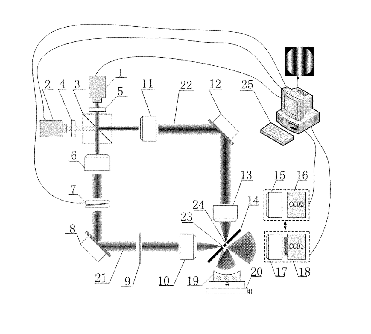
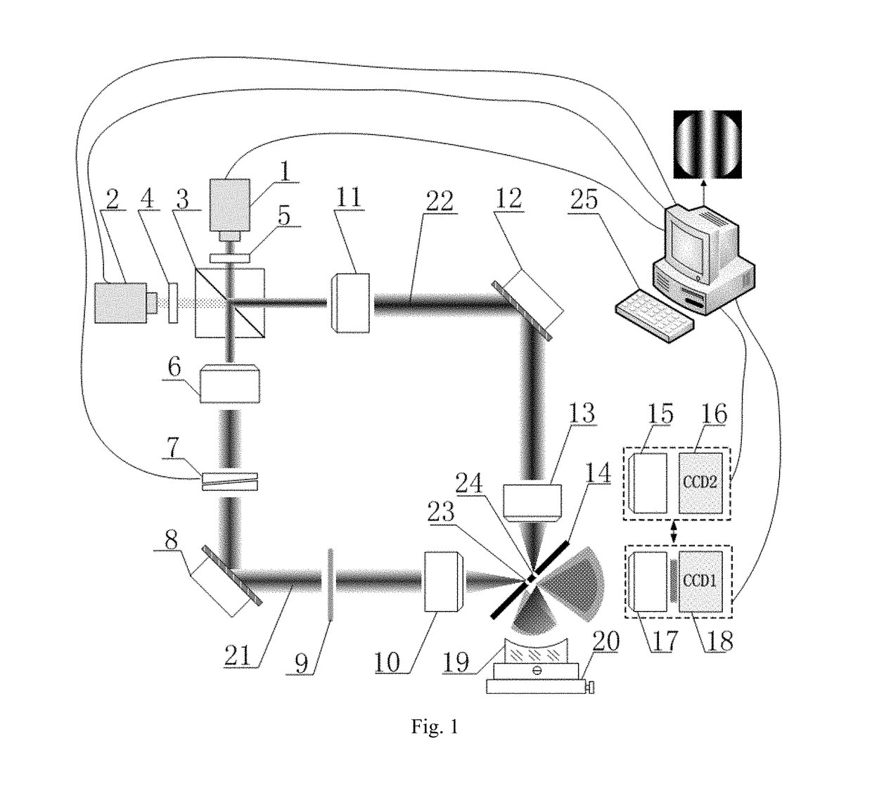
[0058]The inventive principle of the invention is:

[0059]The large numerical aperture phase-shifting dual pinhole diffraction interferometer of present invention adopts a dual pinhole substrate and an illuminating manner of two converged light paths, enabling the separation of reference light passage and test light passage, to prevent the disturbance between the two light paths, which would induce the change of interferogram status during phase-shifting. The small field interferogram optical imaging system is merely aligned with the reference light path / passage to image, so it can avoid the influence of the test light passage to the image, and achieve a large numerical aperture test in a phase-shifting manner. Meanwhile, it adopts multistep optical phase-shifting plate, and changes the thickness of the optical phase-shifting plate within the reference light passage via the lateral movement of the wedge phase-shifting plate, thereby changing the optical path difference between the ref...


PUM


Abstract

The present invention relates to a large numerical aperture phase-shifting dual pinhole diffraction interferometer and its test method, the diffraction interferometer comprises: reference light passage, test light passage and pinhole substrate; wherein, said pinhole substrate comprises test pinhole and reference pinhole; the diffracted wavefront emitted from the test pinhole would be reflected by the optical component to be tested near the pinhole substrate and converge near the reference pinhole, and said diffracted wavefront comprising surface shape information of optical component to be tested, would be reflected by the pinhole substrate and interference with the diffracted wavefront emitted by reference pinhole, forming interference fringes. The large numerical aperture phase-shifting dual pinhole diffraction interferometer of present invention adopts a dual pinhole substrate and a illumination manner with two converged light paths, enabling the separation of the reference light and test light, to prevent the disturbance between the two light paths, which would induce the change of interferogram status during phase-shifting. By using small field interferogram optical imaging system, the present invention avoids the influence of the test light passage, and achieves a large numerical aperture test in a phase-shifting manner

Description

TECHNICAL FIELD[0001]The present invention relates to the technical field of point diffraction interferometer, and particularly relates to a large numerical aperture phase-shifting dual pinhole diffraction interferometer and its test method.BACKGROUND[0002]Due to the unique feature of interference wavefront reference generation technology, point diffraction interferometer become a metrology level optical wavefront test instrument, which is mainly applied in the calibration and measurement of commercial standard lens and in the development of high precision lithography lens.[0003]Currently, there are two kinds of working mechanism of point diffraction interferometer: the first one is as follows: making a pinhole less than 1 micrometer on an optical substrate, which produces a high-precision spherical diffraction wavefront when the light path through said pinhole; using one portion of said wavefront as test light, and another portion as reference light, so that two portions of light i...

Claims


Application Information

Patent Timeline
IPC IPC(8): G01B9/02G01M11/00G01B11/24
CPCG01B9/02038G01B9/02041G01M11/005G01B11/2441G01B9/02072G01M11/0271
Inventor VOZNESENSKIY, NIKOLAYMA, DONGMEIJIN, CHUNSHUIZHANG, HAITAOYU, JIEVOZNESENSKAIA, MARIIAVOZNESENSKAIA, TATIANAZHANG, WENLONG
Owner CHANGCHUN INST OF OPTICS FINE MECHANICS & PHYSICS CHINESE ACAD OF SCI
Why Eureka
Try Eureka