Thin film transistor, manufacturing process for thin film transistor, and laser annealing apparatus

a manufacturing process and technology of thin film transistor, applied in the direction of transistors, electrical devices, semiconductor devices, etc., can solve the problems of increasing the electric field intensity between the electrodes, complicated manufacturing process, increasing etc., to reduce the off-leakage current in the tft, reduce the mobility of electrons, and reduce the crystal grain size

Inactive Publication Date: 2017-08-17
V TECH CO LTD
View PDF2 Cites 8 Cited by
  • Summary
  • Abstract
  • Description
  • Claims
  • Application Information

AI Technical Summary

Benefits of technology

[0009]In view of some of the above problems, it is an object of the present invention to provide a thin film transistor that aims at the structure capable of reducing an off-leakage current through a simple manufacturing process, and a manufacturing process and a laser annealing apparatus for such thin film transistor.
[0013]According to the present invention, the polysilicon thin film in the regions corresponding to the respective source and drain electrodes can have a smaller crystal grain size than that in the channel region between the source and drain electrodes out of the polysilicon thin film only by controlling a laser fluence at the time of applying laser annealing to the amorphous silicon thin film. Accordingly, the mobility of electrons can be lowered in the regions corresponding to the respective source and drain electrodes compared to the channel region, and an off-leakage current in the TFT can be reduced.
[0014]If uniformly annealing the channel region alone, there is a risk that after that annealing treatment, the source and drain electrodes may be formed on the semiconductor layer, not in alignment with the channel region, such offset affects electrical characteristics of the TFT. According to the present invention, however, the crystal grain size of the polysilicon thin film for the semiconductor layer is changed in stages at the regions corresponding to the respective source and drain electrodes and the channel region, whereby the acceptable level of offset can be raised and thus, the TFT can be easily manufactured.

Problems solved by technology

This may cause a problem of increasing electric field intensity between the electrodes and in turn increasing an off-leakage current in the TFT.
To that end, the conventional TFTs require the step of doping impurities into the polysilicon thin film, leading to a complicated manufacturing process and high manufacturing costs.

Method used


Image

  • Thin film transistor, manufacturing process for thin film transistor, and laser annealing apparatus
  • Thin film transistor, manufacturing process for thin film transistor, and laser annealing apparatus
  • Thin film transistor, manufacturing process for thin film transistor, and laser annealing apparatus

Examples


Embodiment Construction

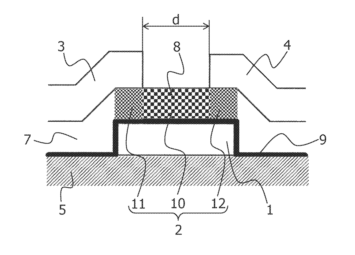
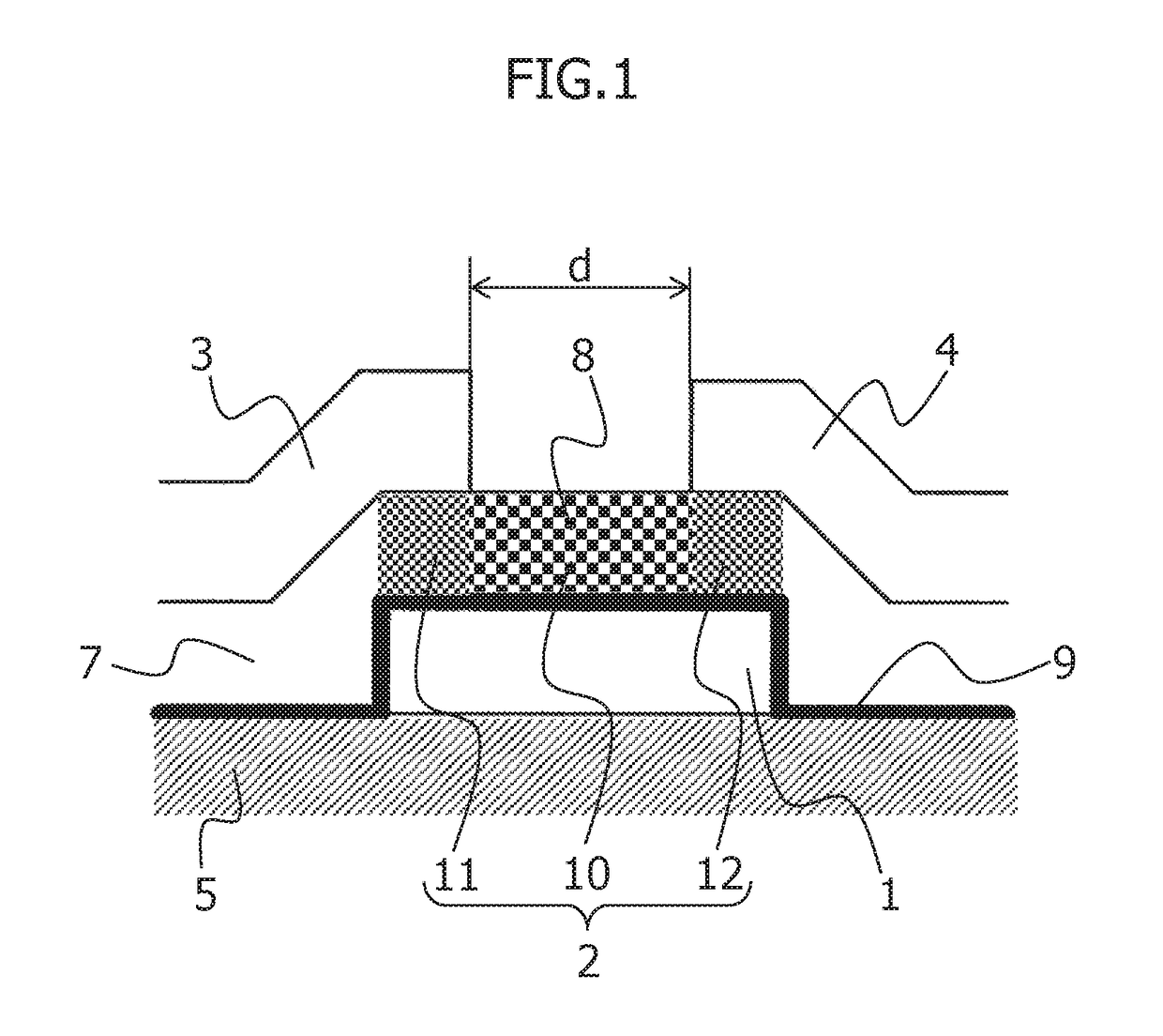
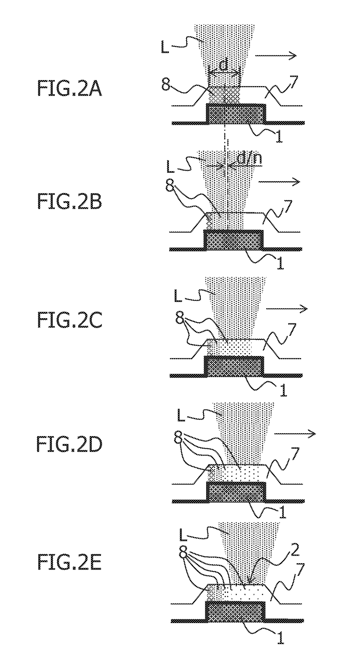
[0025]An embodiment of the present invention will be described in detail below with reference to the accompanying drawings. FIG. 1 is a cross-sectional view showing a thin film transistor according to an embodiment of the present invention. The thin film transistors (TFTs) are provided at intersections between plural data lines and gate lines that crisscross each other on a TFT substrate so as to drive pixel electrodes of a display. The respective TFTs are composed of a gate electrode 1, a semiconductor layer 2, a source electrode 3, and a drain electrode 4.

[0026]The gate electrodes 1 are formed in a matrix at regular array pitches on the substrate 5 in the form of transparent glass and also are electrically connected to plural gate lines 6 (see FIGS. 3A to 3E) extending in parallel to the horizontal direction of the substrate 5 so as to receive scanning information from a gate drive circuit provided outside a display region.

[0027]The semiconductor layer 2 is formed over the gate el...


PUM

PropertyMeasurementUnit
source-drain widthaaaaaaaaaa
wavelengthaaaaaaaaaa

Abstract

The present invention provides a thin film transistor including a gate electrode, a source electrode, a drain electrode, and a semiconductor layer, which are laminated on a substrate. The semiconductor layer is a polysilicon thin film. The polysilicon thin film in regions corresponding to the source electrode and the drain electrode has a smaller crystal grain size than that of the polysilicon thin film in a channel region between the source electrode and the drain electrode.

Description

CROSS-REFERENCE TO RELATED APPLICATION[0001]This application is a continuation application of PCT / JP2015 / 082554, filed on Nov. 19, 2015, the entirety of which is incorporated herein by reference.BACKGROUND OF THE INVENTION[0002]1. Field of the Invention[0003]The present invention relates to a thin film transistor including a semiconductor layer in the form of a polysilicon thin film, and more particularly to a thin film transistor that aims at the structure capable of reducing an off-leakage current through a simple manufacturing process, and a manufacturing process and a laser annealing apparatus for such thin film transistor.[0004]2. Description of Related Art[0005]Thin film transistors (hereinafter referred to as “TFTs”) generally have the structure including a gate electrode, a source electrode, a drain electrode, and a semiconductor layer, which are laminated on a substrate. Of those, a TFT using a polysilicon thin film as the semiconductor layer shows high electron mobility an...

Claims


Application Information

Patent Timeline
Patent Type & Authority Applications(United States)
IPC IPC(8): H01L29/786H01L21/02H01L21/67H01L29/66
CPCH01L29/78678H01L29/78618H01L21/67115H01L21/02675H01L29/66765H01L27/1281H01L29/04H01L29/78621H01L21/20H01L21/268H01L21/324H01L29/6675H01L29/786
Inventor MIZUMURA, MICHINOBUHATANAKA, MAKOTOKIGUCHI, TETSUYA
Owner V TECH CO LTD
Why Eureka
Try Eureka