Method of Producing Transition Metal Dichalcogenide Layer

a technology of transition metal dichalcogenide and dichalcogenide layer, which is applied in the direction of coating, metallic material coating process, chemical vapor deposition coating, etc., can solve the problems of graphene losing much of its attraction as alternative mos channel material, cmos scaling beyond the 12 nm technology node only being possible, and tiny flakes of only few micrometers

Active Publication Date: 2017-08-31
INTERUNIVERSITAIR MICRO ELECTRONICS CENT (IMEC VZW) +1
View PDF4 Cites 316 Cited by
  • Summary
  • Abstract
  • Description
  • Claims
  • Application Information

AI Technical Summary

Benefits of technology

[0007]It is an object of embodiments of the present invention to provide a good method for producing at least one two-dimensional transition metal dichalcogenide layer on a semiconductor, e.g. silicon substrate. A “layer of a 2D tran...

Problems solved by technology

However, the continuation of CMOS scaling beyond the 12 nm technology node will only be possible if device engineers replace the traditional silicon channel of e.g. a transistor by more powerful semiconductor materials.
Measures to open up the bandgap (‘chemical functionalization’) are known but deteriorate at the same time its mobility, hence graphene is losing much of its attraction as alternative MOS channel material.
It is a major challenge however to produce MX2 layers in relatively large areas and/or with the desired orientation (e.g. substantially parallel to the substrate) so as to make them fit for integration into high-volume semiconductor manufacturing on e.g. 300 or 450 mm semiconductor substrates, e.g. silicon wafers.
This results in tiny flakes of only few micrometer size.
Many approaches have been studied to produce samples of layered MX2, but as far as known to the inv...

Method used


Image

  • Method of Producing Transition Metal Dichalcogenide Layer
  • Method of Producing Transition Metal Dichalcogenide Layer
  • Method of Producing Transition Metal Dichalcogenide Layer

Examples


Embodiment Construction

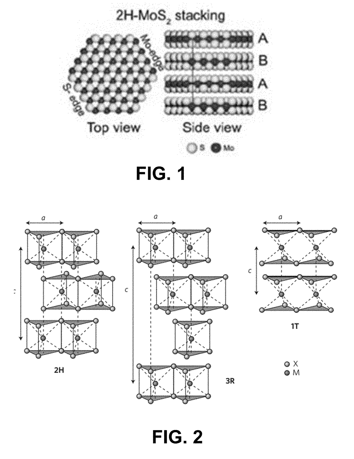
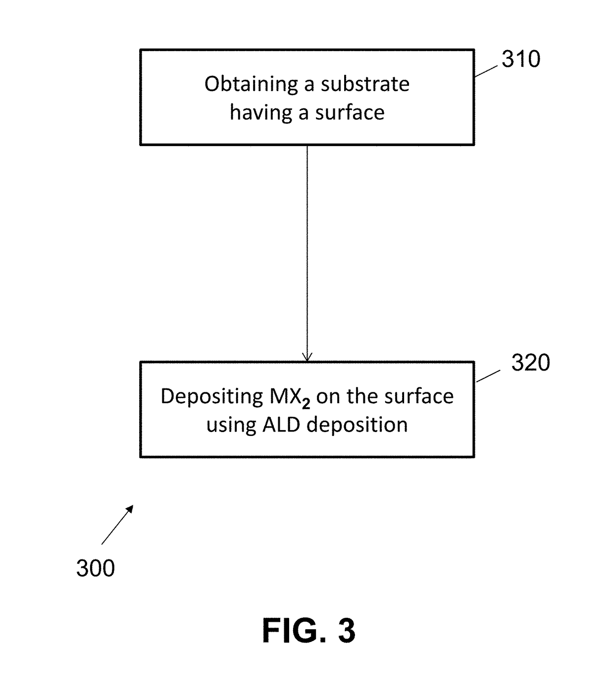
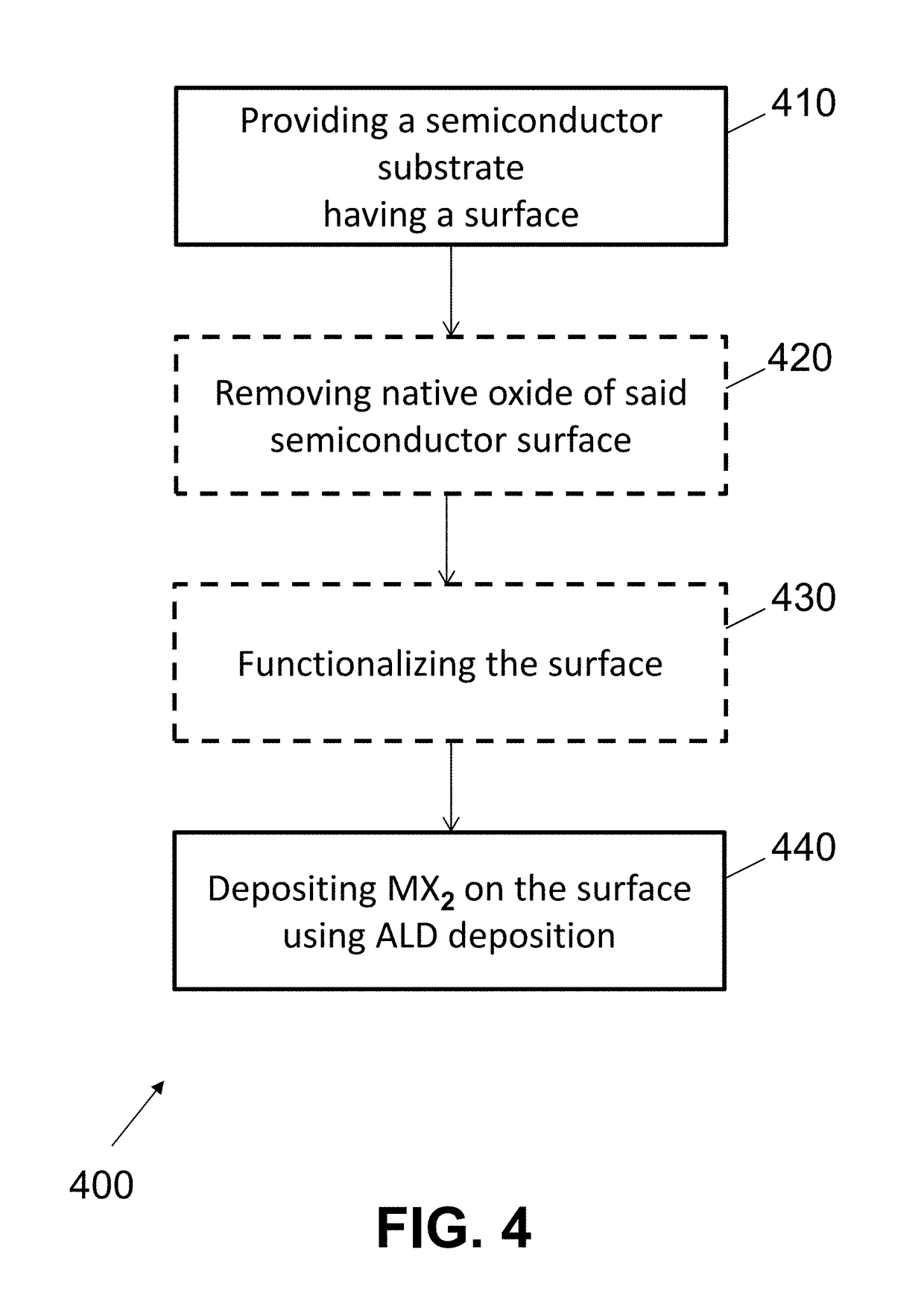
[0060]The present invention will be described with respect to particular embodiments and with reference to certain drawings but the invention is not limited thereto but only by the claims. The drawings described are only schematic and are non-limiting. In the drawings, the size of some of the elements may be exaggerated and not drawn on scale for illustrative purposes. The dimensions and the relative dimensions do not correspond to actual reductions to practice of the invention.

[0061]The terms first, second and the like in the description and in the claims are used for distinguishing between similar elements and not necessarily for describing a sequence, either temporally, spatially, in ranking or in any other manner. It is to be understood that the terms so used are interchangeable under appropriate circumstances and that the embodiments of the invention described herein are capable of operation in other sequences than described or illustrated herein.

[0062]Moreover, the terms top, ...


PUM

PropertyMeasurementUnit
Temperatureaaaaaaaaaa

Abstract

Method of producing one or more transition metal dichalcogenide (MX2) layers on a substrate, comprising the steps of: obtaining a substrate having a surface and depositing MX2 on the surface using ALD deposition, starting from a metal halide precursor and a chalcogen source (H2X), at a deposition temperature of about 300° C. Suitable metals are Mo and W, suitable chalcogenides are S, Se and Te. The substrate may be (111) oriented. Also mixtures of two or more MX2 layers of different compositions can be deposited on the substrate, by repeating at least some of the steps of the method.

Description

FIELD OF THE INVENTION[0001]The invention relates to methods of producing transition metal dichalcogenide layers on a substrate. The invention relates in particular to methods of producing a limited number of layers, for instance less than seven layers of transition metal dichalcogenides on a relatively large substrate.BACKGROUND OF THE INVENTION[0002]As is well known, the number of transistors on integrated circuits approximately doubles every two years, in accordance with Moore's Law. However, the continuation of CMOS scaling beyond the 12 nm technology node will only be possible if device engineers replace the traditional silicon channel of e.g. a transistor by more powerful semiconductor materials. High carrier mobility materials such as germanium and / or compound semiconductor materials have now matured to an industrial development level, but even these material reach their limits in view of very small devices.[0003]A next generation of materials are two-dimensional materials su...

Claims


Application Information

Patent Timeline
IPC IPC(8): H01L21/02C23C16/56C23C16/455C23C16/02C23C16/30
CPCH01L21/02568C23C16/02C23C16/305C23C16/45553C23C16/56H01L21/02658H01L21/0262H01L21/02068H01L21/02664H01L21/02381H01L21/02488H01L21/02433H01L21/02052H01L21/02661
Inventor CAYMAX, MATTYHEYNE, MARKUSDELABIE, ANNELIES
Owner INTERUNIVERSITAIR MICRO ELECTRONICS CENT (IMEC VZW)
Why Eureka
Try Eureka