Real-time stimulation artifact suppression for simultaneous electrophysiological electrical stimulation and recording
- Summary
- Abstract
- Description
- Claims
- Application Information
AI Technical Summary
Benefits of technology
Problems solved by technology
Method used
Image
Examples
embodiment 30
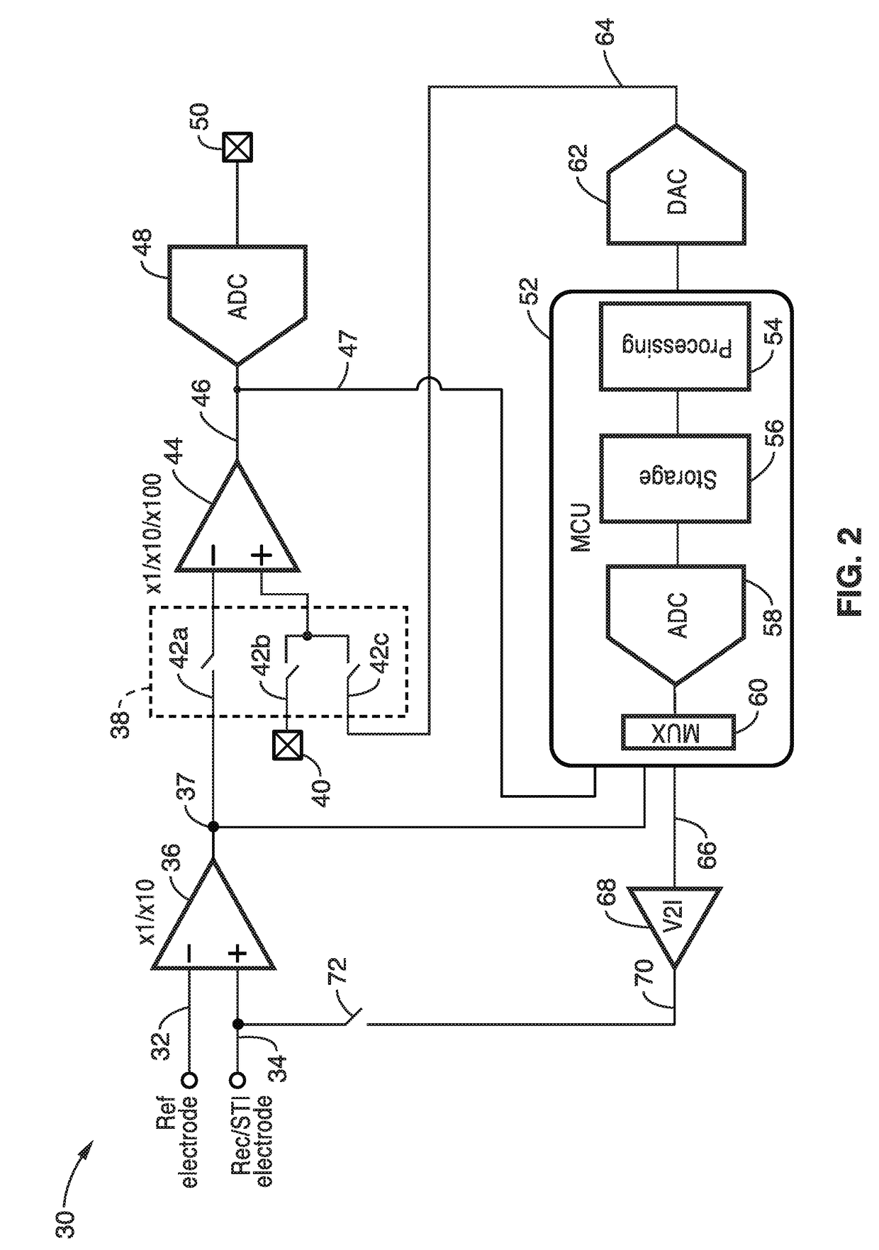
[0040]FIG. 2 illustrates an embodiment 30 for the disclosed artifact removal / reduction system. In general the system comprises at least two input amplifiers and a stimulus output amplifier which are controlled by control circuitry. More particularly an implementation of the system is seen in the figure comprising two amplification stages 36, 44, an analog-to-digital converter (ADC) 48, a digital-to-analog converter (DAC) 62, a stimulator 68 with output 34, and a microcontroller unit (MCU) 52 (or other means of electronic control, such as any type of CPU or DSP, FPGAs, gate arrays, logic arrays, or similar circuits utilized separately or in combination) for controlling stimulus outputs, measurement collection and artifact suppression.
[0041]Under normal operation, two inputs of the first amplifier 36 are connected to the working electrode 34 and the reference electrode 32 to pick up and amplify the neural signal. It should be appreciated that multiple amplifiers may be alternatively u...
embodiment 90
[0047]FIG. 3A and FIG. 3B illustrate embodiments showing Phase 1 and Phase 2 paths. In FIG. 3A an embodiment 90 is seen showing a Phase 1 path 92 with the processor controlling the stimulator to generate a stimulus into the tissue to acquire the first artifact template. The recording electrode 34 is connected to the stimulator signal 70 from amplifier 68 through switch 72, while the output of the first amplifier 36 is configured as a unity gain buffer directed to a programmable second stage amplification 94. It will be readily recognized that the elements depicted in this Phase 2 path diagram represent different connections of those elements shown in FIG. 2.
embodiment 110
[0048]FIG. 3B illustrates an embodiment 110 showing a Phase 2 path 116 in which calibration of the artifact template is performed. The second amplifier 44 is activated and configured as a unity-gain buffer and a second stimulus 70 is sent to the electrode model 34 during artifact acquisition. It should be noted that output 66 comprises one or more control signals to the voltage-to-current (V2I) (stimulator), with output 64 being the actual DAC output, sent to the input of amplifier 44. The stored artifact is converted to an analog waveform via DAC 62 and passed 64 to the positive terminal of the second amplifier 44. Thus, the artifact signal and the reconstructed artifact are subsequently subtracted inside amplifier 44 with its output 46 digitized by ADC 112 circuit and stored in the MCU. It should be appreciated that multiple calibration passes may be performed as desired, such as until a desire accuracy is verified. In addition, the artifact templates can be adjusted in any desire...
PUM
 Abstract
Description
Claims
Application Information


