Semiconductor memory devices and methods of operating the same

Active Publication Date: 2017-10-05
SAMSUNG ELECTRONICS CO LTD
View PDF2 Cites 10 Cited by
  • Summary
  • Abstract
  • Description
  • Claims
  • Application Information

AI Technical Summary

Benefits of technology

The patent text describes a semiconductor memory device that can reduce power consumption without taking up more space. This is achieved by reducing the number of data strobe signals used when the frequency of the clock signal is smaller than or equal to the reference frequency, compared to the number of signals used when the frequency of the clock signal is greater than the reference frequency. This helps to lower the overall current consumption of the memory device.

Problems solved by technology

Power consumption of the synchronous semiconductor memory device increases as the amount of data increases.

Method used


Image

  • Semiconductor memory devices and methods of operating the same
  • Semiconductor memory devices and methods of operating the same
  • Semiconductor memory devices and methods of operating the same

Examples


Embodiment Construction

[0029]Various exemplary embodiments will be described more fully hereinafter with reference to the accompanying drawings, in which some exemplary embodiments are shown.

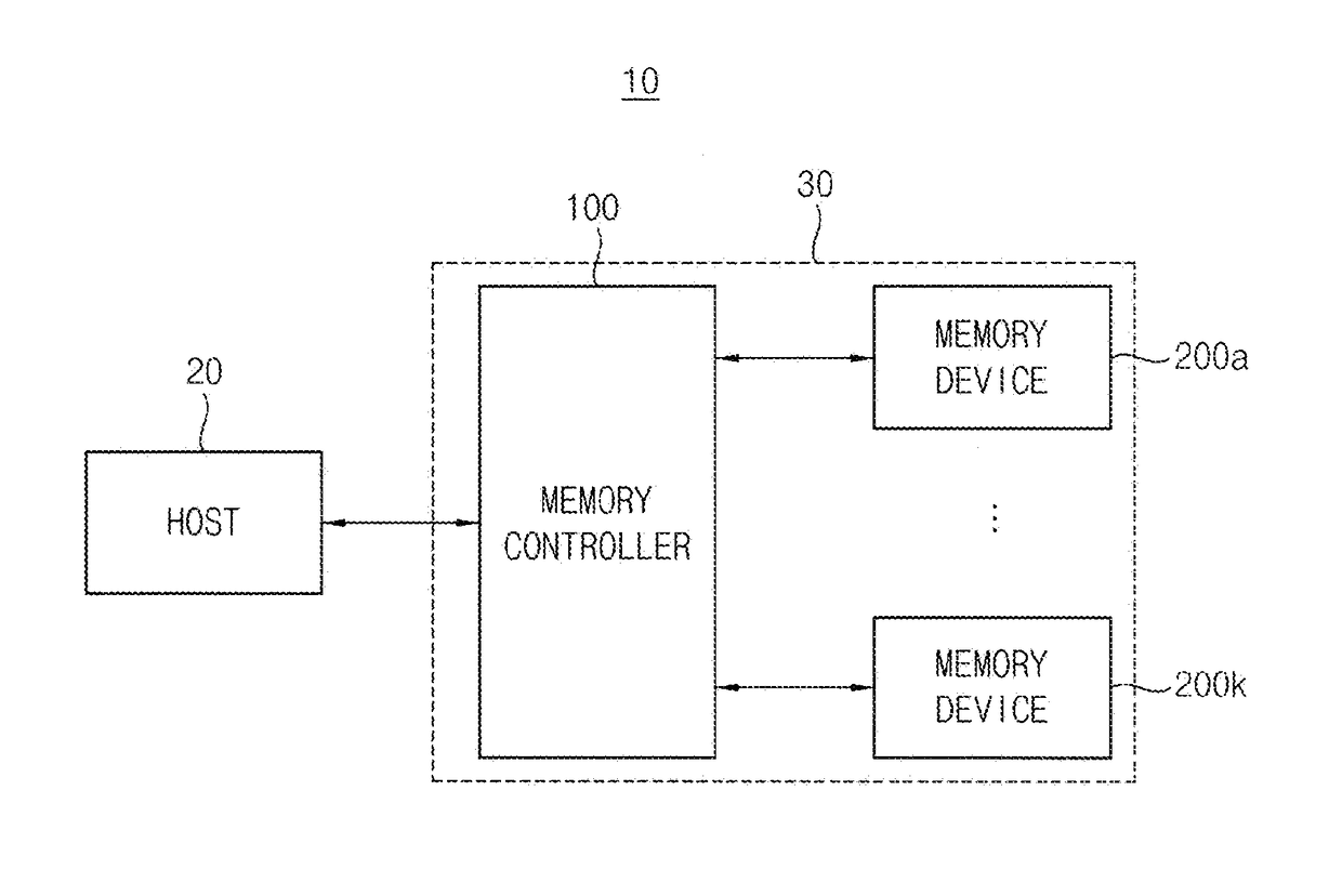
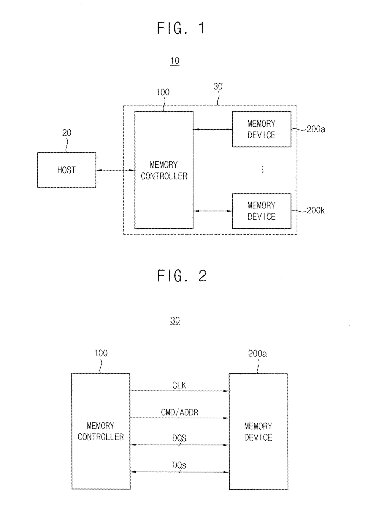
[0030]FIG. 1 is a block diagram illustrating an electronic memory system according to exemplary embodiments.

[0031]Referring to FIG. 1, an electronic system 10 may include a host 20 and a memory system 30. The memory system 30 may include a memory controller 100 and multiple semiconductor memory devices 200a˜200k.

[0032]The host 20 may communicate with the memory system 30 through various interface protocols such as Peripheral Component Interconnect-Express (PCI-E), Advanced Technology Attachment (ATA), Serial ATA (SATA), Parallel ATA (PATA), or serial attached SCSI (SAS). In addition, the host 20 may also communicate with the memory system 30 through interface protocols such as Universal Serial Bus (USB), Multi-Media Card (MMC), Enhanced Small Disk Interface (ESDI), or Integrated Drive Electronics (IDE).
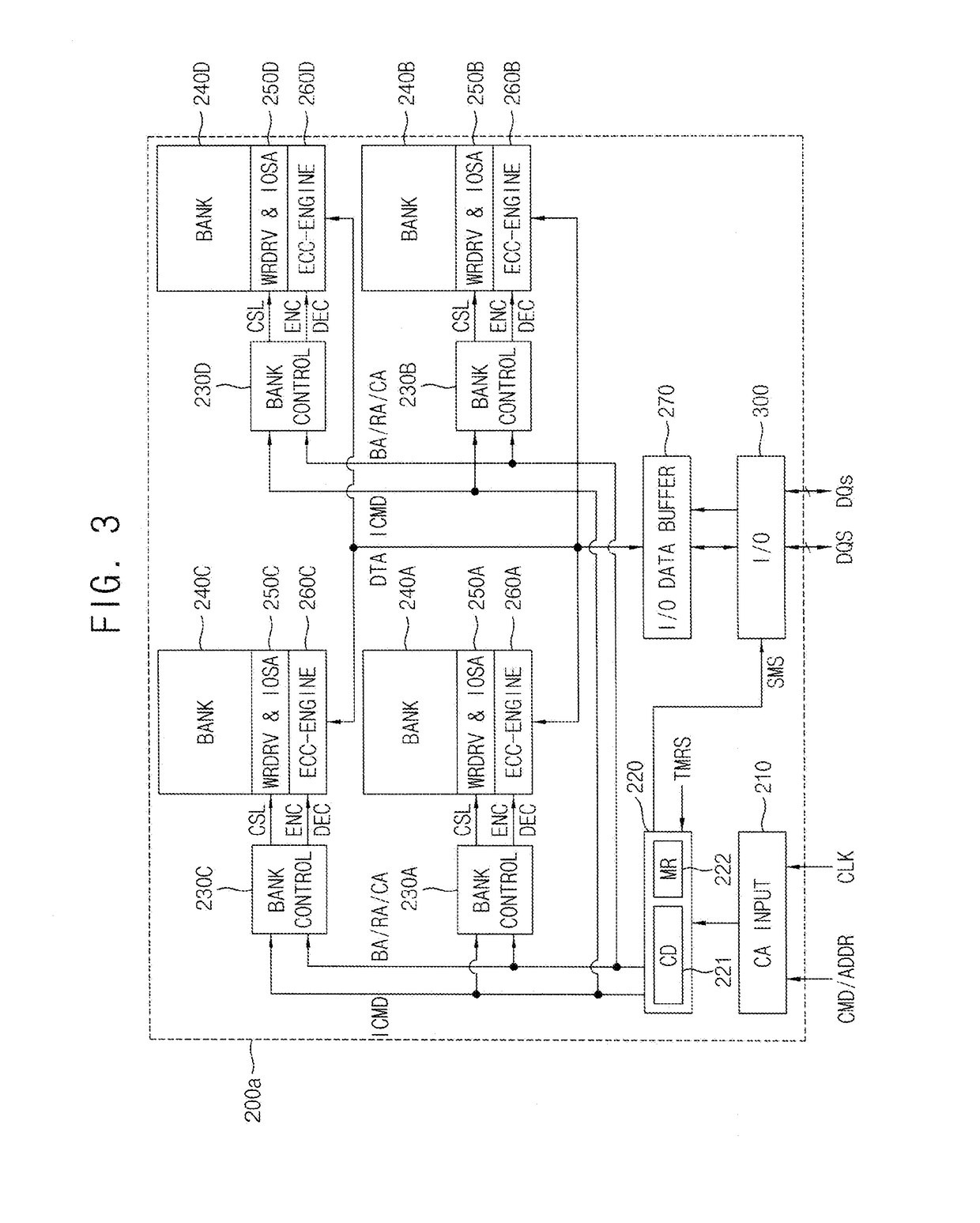
[0033]The memo...


PUM


Abstract

A semiconductor memory device includes a memory cell array and a control logic circuit. The control logic circuit controls access to the memory cell array based on a command and an address. The semiconductor memory device performs a write operation to write data in the memory cell array and performs a read operation to read data from the memory cell array in synchronization with a clock signal from an external memory controller. The semiconductor memory device performs the write operation and the read operation in different data strobe modes in which the semiconductor memory device uses different numbers of data strobe signals according to a frequency of the clock signal.

Description

CROSS-REFERENCE TO RELATED APPLICATION(S)[0001]This application claims priority under 35 U.S.C. §119 to Korean Patent Application No. 10-2016-0037322, filed on Mar. 29, 2016 in the Korean Intellectual Property Office, the disclosure of which is incorporated by reference herein in its entirety.BACKGROUND1. Technical Field[0002]The present disclosure relates to memory devices. More particularly, the present disclosure relates to semiconductor memory devices and methods of operating the same.2. Background Information[0003]In general, a semiconductor memory device such as a double data rate synchronous dynamic random access memory (DDR SDRAM) includes tens of millions of memory cells, and stores and outputs data in response to a command requested from a chipset. That is, if the chipset requests a write operation to the semiconductor memory device, the semiconductor memory device stores data on a memory cell corresponding to an address inputted from the chipset. If the chipset requests a...

Claims


Application Information

Patent Timeline
IPC IPC(8): G11C11/4096G06F1/08G06F1/12G11C11/4076G11C8/18
CPCG11C11/4096G11C11/4076G06F1/08G06F1/12G11C8/18G11C7/1063G11C7/109G11C7/222G11C7/1003G11C7/1066G11C7/1093G11C17/16G11C29/023G11C2029/0411G11C11/409G11C7/1006G11C7/1051G11C7/1084
Inventor RYU, SEUNG-WOOKANG, SANG-KYU
Owner SAMSUNG ELECTRONICS CO LTD
Why Eureka
Try Eureka