Engineered etched interfaces for high performance junctions

Inactive Publication Date: 2017-10-05
IBM CORP
View PDF0 Cites 1 Cited by
  • Summary
  • Abstract
  • Description
  • Claims
  • Application Information

AI Technical Summary

Benefits of technology

[0006]Use of such a method for surface preparation can take advantage of its self-limiting quality for a high degree of control preventing damage in a sensitive channel or contact. The method can also take advantage of its selectivity for stopping on the semiconductor layer. Furthermore, the method can be used as an additional knob in CMOS integration to r

Problems solved by technology

This is particularly challenging for high-mobility semiconductors (such as InGaAs & SiGe) for which a low quality native oxide readily forms after air exposure so that wet chemistry is not sufficient to condition the substrate appropriately.
This also adds a queue-time dependence between wet chemical treatment and dielectric gate or metal contact deposition so that the integration is rendered non-practical in a manufacturing setting.
On III-V substrates, proposed solutions are limited due to, for example, the small process compatibility window (e.g. temperature up to 400 C).
Sul

Method used


Image

  • Engineered etched interfaces for high performance junctions
  • Engineered etched interfaces for high performance junctions
  • Engineered etched interfaces for high performance junctions

Examples


Embodiment Construction

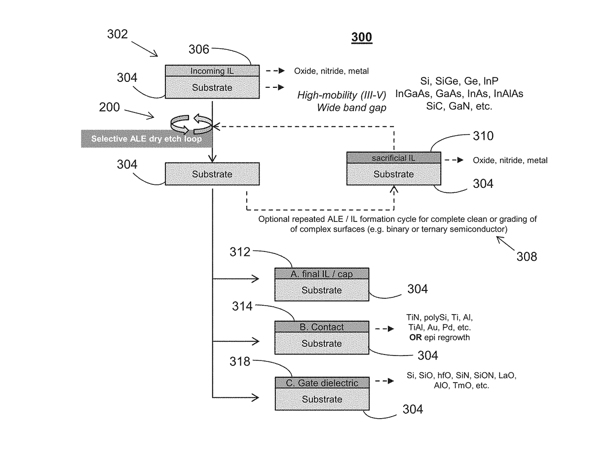
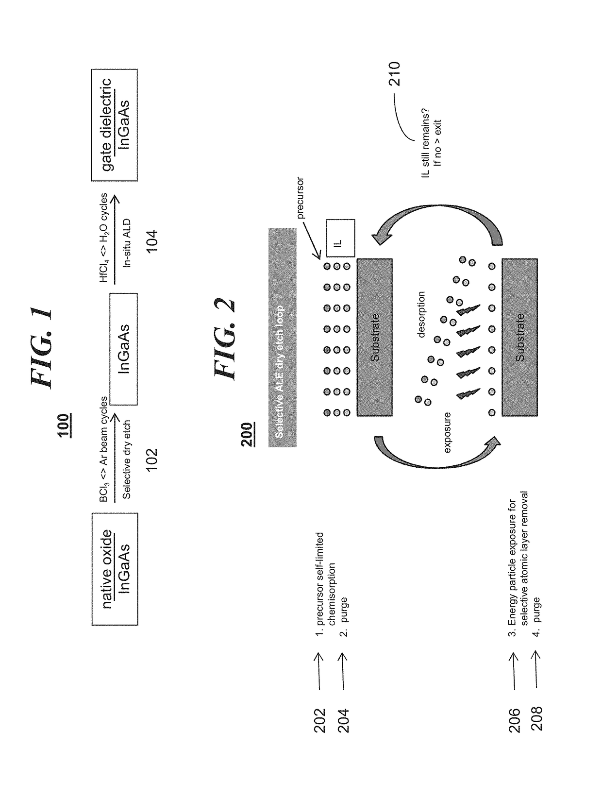
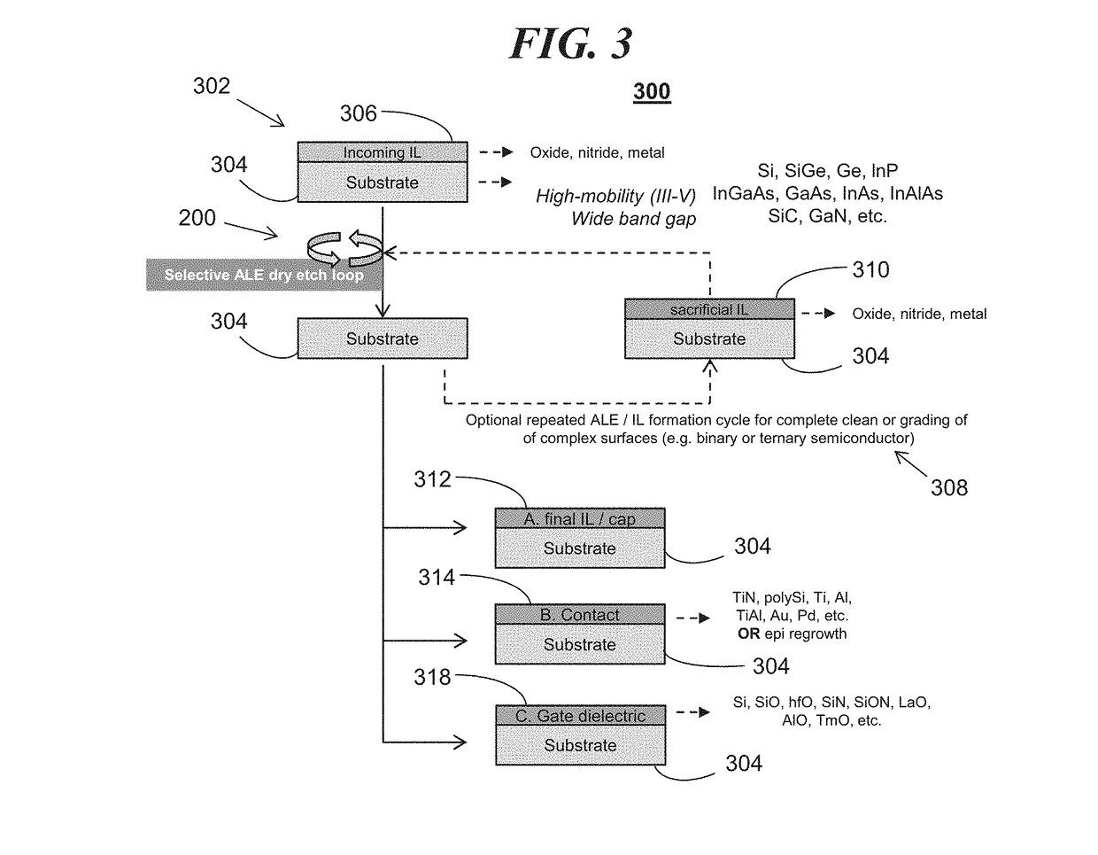
[0014]It is to be understood that the present disclosure will be described in terms of a given illustrative example process for surface conditioning of semiconductor interfaces, junctions, and contacts. However, other semiconductor architectures, structures, substrate materials, and process features and steps may be varied within the scope of the present disclosure.

[0015]It will also be understood that when an element such as a layer, region or substrate is referred to as being “on” or “over” another element, it can be directly on the other element or intervening elements may also be present. In contrast, when an element is referred to as being “directly on” or “directly over” another element, there are no intervening elements present. It will also be understood that when an element is referred to as being “connected” or “coupled” to another element, it can be directly connected or coupled to the other element or intervening elements may be present. In contrast, when an element is r...


PUM


Abstract

Various methods for fabricating a semiconductor device by selective in-situ cleaning of a target surface of a semiconductor substrate by selective dry surface atomic layer etching of the target surface film, selectively removing one or more top layers of atoms from the target surface film of the semiconductor substrate. The selective in-situ cleaning of a target surface can be followed by deposition on the cleaned target surface such as to form a cap layer, a conductive contact layer, or a gate dielectric layer.

Description

BACKGROUND OF THE INVENTION[0001]The present disclosure generally relates to the field of semiconductors, and more particularly relates to a method of fabricating semiconductor interfaces, junctions, and contacts.[0002]Obtaining a pristine and / or passivated semiconductor surface without damaging the bulk of the film is critical to gate stack and contact formation in order to improve transfer characteristics (mobility, sub-threshold slope, etc.) and reduce resistivity, respectively.[0003]This is particularly challenging for high-mobility semiconductors (such as InGaAs & SiGe) for which a low quality native oxide readily forms after air exposure so that wet chemistry is not sufficient to condition the substrate appropriately. This also adds a queue-time dependence between wet chemical treatment and dielectric gate or metal contact deposition so that the integration is rendered non-practical in a manufacturing setting.[0004]On III-V substrates, proposed solutions are limited due to, fo...

Claims


Application Information

Patent Timeline
IPC IPC(8): H01L21/28H01L29/51H01L21/3213H01L21/311H01L21/02
CPCH01L21/28158H01L21/0217H01L21/02065H01L21/02074H01L21/32135H01L21/0228H01L29/517H01L21/28026H01L21/02178H01L21/02181H01L21/02192H01L21/02123H01L21/02164H01L21/02167H01L21/31116H01L21/02301H01L21/28264
Inventor BRUCE, ROBERT L.MIYAZOE, HIROYUKIROZEN, JOHN
Owner IBM CORP
Why Eureka
Try Eureka