

Solid state imaging device and manufacturing method therefor
- Summary
- Abstract
- Description
- Claims
- Application Information
AI Technical Summary
Benefits of technology
Problems solved by technology
Method used
Image

Examples
embodiment 1
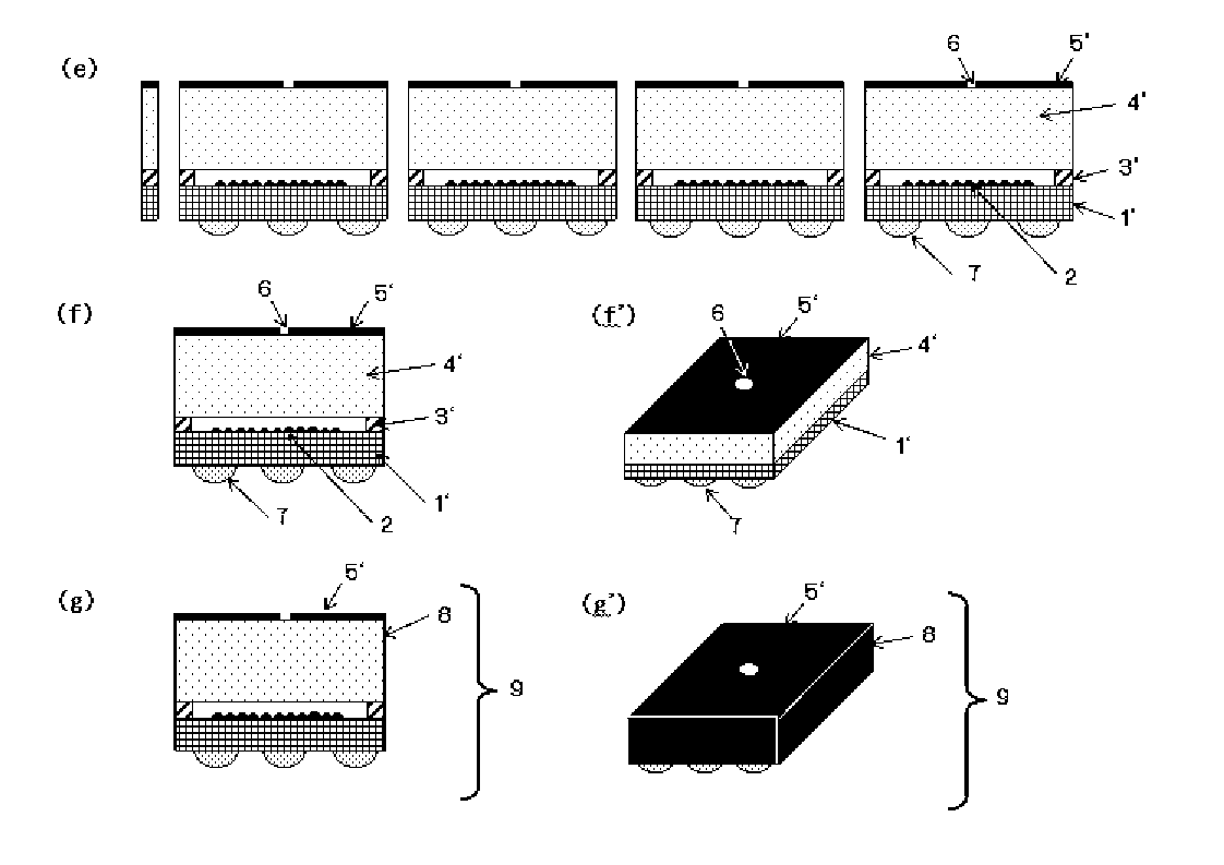
[0037]A method for manufacturing a wafer-level pinhole camera module according to a first embodiment of the present invention will be described with reference to FIG. 1(a) to FIG. 1(f). FIG. 1(a) shows an image sensor wafer 1 formed on a semiconductor substrate, with a microlens 2 formed over pixels of a photosensitive portion of the surface of each sensor. In order to manufacture a wafer-level camera module, an adhesive material 3 is formed in areas other than the photosensitive portion of each sensor, and a cover glass wafer 4 is attached to the image sensor wafer 1 via the adhesive material 3 therebetween so as to cover the image sensor wafer 1.
[0038]As shown in FIG. 1(a), the microlens 2 is formed over pixels in the photosensitive portion on the surface of each sensor. The adhesive material 3 is formed in areas other than the photosensitive portion of each sensor, and the cover glass wafer 4 being flat with no surface irregularities, is attached thereto with the adhesive materia...
embodiment 2
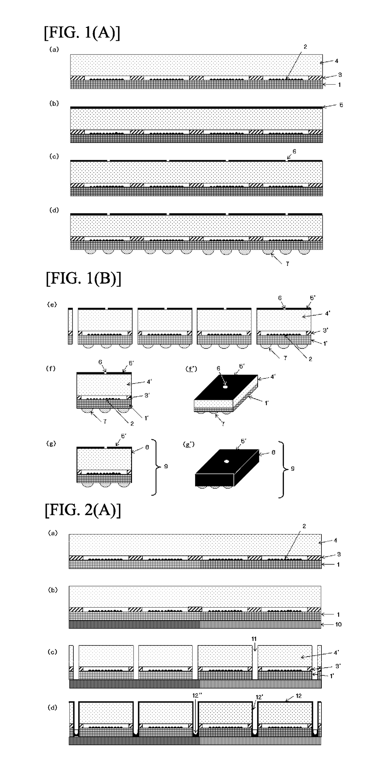
[0050]A method for manufacturing a wafer-level pinhole camera module according to a second embodiment of the present invention will be described with reference to FIG. 2(a) to FIG. 2(j). In FIG. 2(a), as in FIG. 1(a), the image sensor wafer 1 is formed on a semiconductor substrate, the microlens 2 is formed over pixels in the photosensitive portion on the surface of each sensor, the adhesive material 3 is formed in areas other than the photosensitive portion of each sensor, and the cover glass wafer 4 is attached to the image sensor wafer 1 via the adhesive material 3 so as to cover the image sensor wafer 1.
[0051]In the next step, as shown in FIG. 2(b), a dicing tape 10 is attached to the reverse surface of the image sensor wafer 1. The dicing tape 10 has an adhesive material (not shown) formed thereon for holding the wafer when the wafer is diced.
[0052]In the next step, as shown in FIG. 2(c), blade dicing is done along dicing areas (not shown) for severing the image sensor wafer 1 ...
embodiment 3
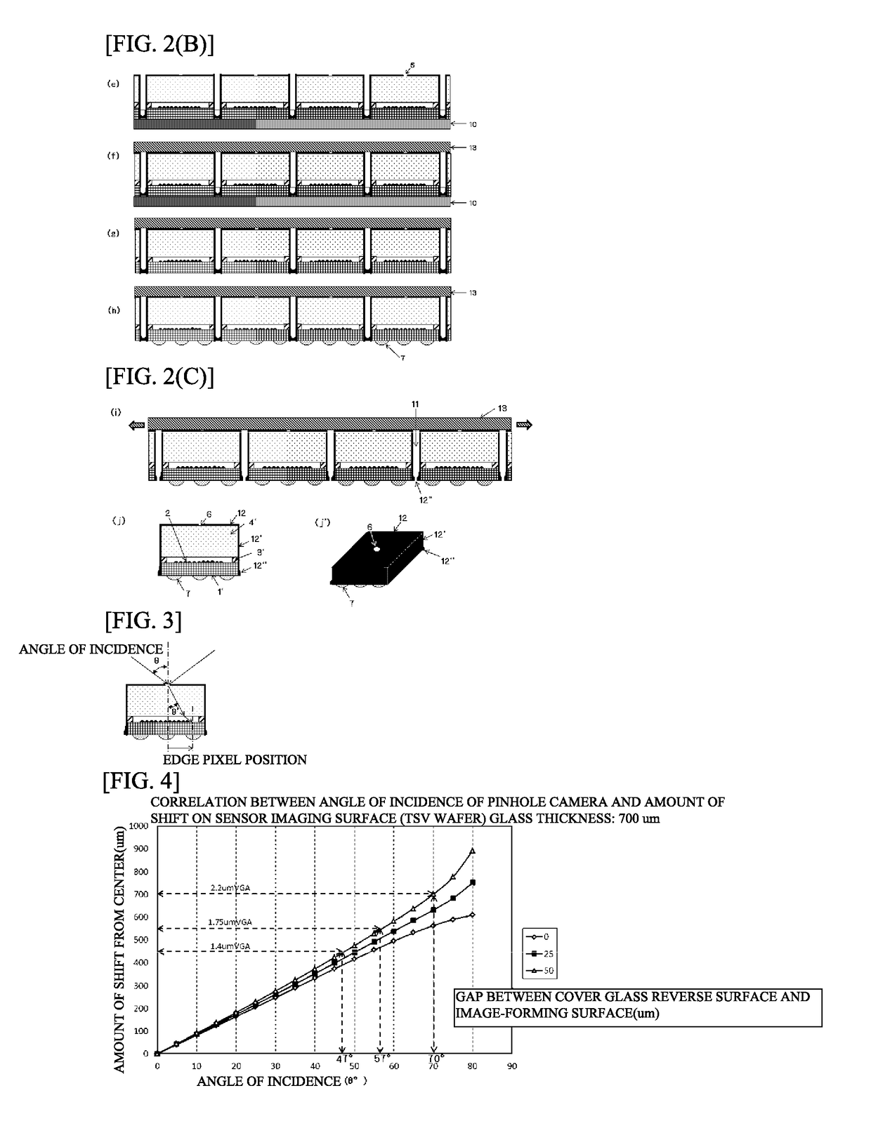
[0066]A wafer-level pinhole camera module according to a third embodiment of the present invention will now be described with reference to FIG. 5(a) to FIG. 5(d). The third embodiment is a wafer-level pinhole camera suitable for stereoscopic camera applications.
[0067]FIG. 5(a), as is FIG. 2(i), is a cross sectional structure diagram after the expand tape 13 is literally expanded to increase the width of the dicing groove 11 in the gap portion between the cover glasses 4′ and the image sensor chips 1′, thereby severing the bottom portion light-blocking material 12″ on the dicing groove bottom portion. A difference from FIG. 2(i′) is that the severing is done as if two adjacent image sensor chips were a single image sensor chip.
[0068]The structure of the severed pinhole camera module is as shown in FIG. 5(b). The light-blocking material 12 is present on the top surface, and two openings 6 are formed in the light-blocking material 12 with an interval therebetween that is generally equi...
PUM
 Abstract
Description
Claims
Application Information