Discrete power switching devices with reduced common source inductance

a technology of common source inductance and power switching device, which is applied in the direction of electronic switching, electronic commutator, pulse technique, etc., can solve the problems of limiting efficiency and creation, increasing switching losses, and limiting switching speed, so as to avoid the reduction of switching speed and increase switching losses

Active Publication Date: 2017-12-07
FORD GLOBAL TECH LLC
View PDF3 Cites 6 Cited by
  • Summary
  • Abstract
  • Description
  • Claims
  • Application Information

AI Technical Summary

Benefits of technology

[0010]In one aspect of the invention, an apparatus is providing for switching a discrete power device. The power device has a gate signal path via a gate pin and a power signal path via first and second power pins, wherein the gate signal path and the power signal path have a first mutual inductance. A circuit board apparatus provides a gate wiring loop juxtaposed with the power signal path, wherein the gate wiring loop and the power signal path have a second mutual inductance substantially canceling the first mutual inductance. The resulting reduction in common source inductance avoids the reductions in switching speed and the increased switching losses otherwise introduced by the common source inductance.

Problems solved by technology

The IGBTs and their reverse-recovery diodes have associated switching losses which must be minimized in order to limit loss of efficiency and creation of waste heat.
The voltage induced across the common source inductance modifies the gate voltage in a manner that limits the on / off switching times and increases switching losses.
With new generations of power devices (e.g., CoolMOS, SiC, and GaN devices) becoming faster and faster, the common source inductance dramatically limits the switching speed and increases switching losses.

Method used


Image

  • Discrete power switching devices with reduced common source inductance
  • Discrete power switching devices with reduced common source inductance
  • Discrete power switching devices with reduced common source inductance

Examples


Embodiment Construction

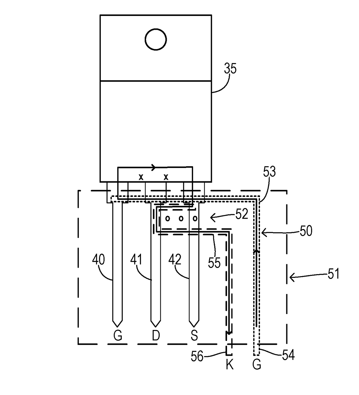
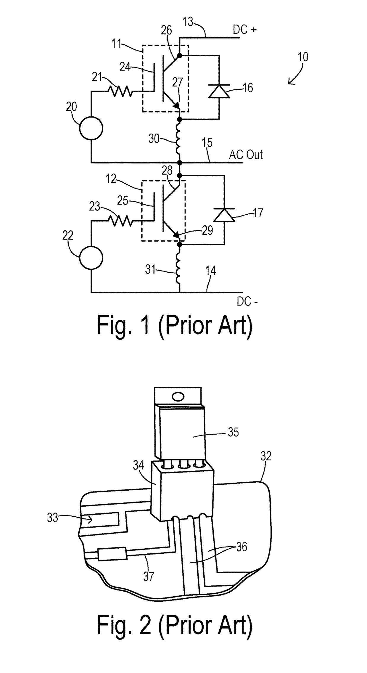
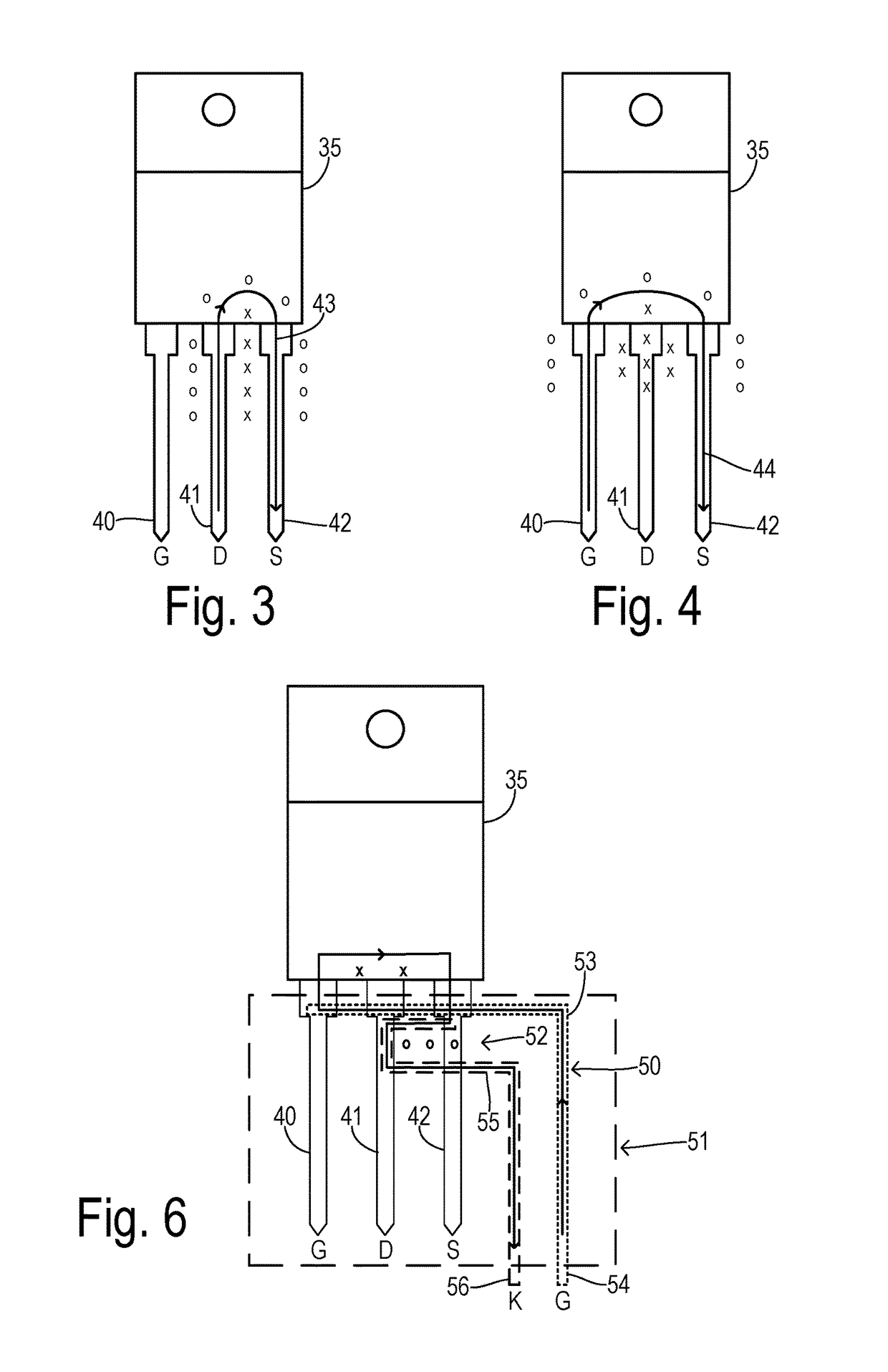
[0024]Devices 11 and 12 have gate drivers 20 and 22 with respective gate coupling resistors 21 and 23 for driving respective gate terminals 24 and 25. Power output terminals 26 and 27 of device 11 and power output terminals 28 and 29 of device 12 are collector and emitter terminals when using IGBTs and are drain and source terminals when using a power MOSFET, for example. The inherent parasitic common source inductance (i.e., the mutual inductance that couples the gate current with the main device output current) is represented by inductances 30 and 31. There may be many contributors to the common source inductance including factors both inside and outside devices 11 and 12. In particular, the mutual inductance arising within devices 11 and 12 has become an increasingly significant disadvantage in the prior art.

[0025]The power switching devices of the present invention may often be mounted to a printed circuit board (PCB) using a socket as shown in FIG. 2. A PCB 32 carrying traces 3...


PUM


Abstract

Routing of a gate signal for controlling a discrete power switching device (such as in an inverter for an electric vehicle drive) is configured to compensate for the common source inductance inherent in the switching device as a result of its integrated circuit packaging. The power device has a gate signal path via a gate pin and a power signal path via first and second power pins, wherein the gate signal path and the power signal path have a first mutual inductance. A circuit board apparatus provides a gate wiring loop juxtaposed with the power signal path, wherein the gate wiring loop and the power signal path have a second mutual inductance substantially canceling the first mutual inductance. The resulting reduction in common source inductance avoids the reductions in switching speed and the increased switching losses otherwise introduced by the common source inductance.

Description

CROSS REFERENCE TO RELATED APPLICATIONS[0001]Not Applicable.STATEMENT REGARDING FEDERALLY SPONSORED RESEARCH[0002]Not Applicable.BACKGROUND OF THE INVENTION[0003]The present invention relates in general to reducing the effects of common source inductance in discrete semiconductor power switching devices, and, more specifically, to inverter drive systems for electrified vehicles using discrete power switching devices with fast switching times and low losses.[0004]Various types of semiconductor power switching devices have been introduced for high-voltage, high-power electronic switching applications such as power MOSFETs and insulated gate bipolar transistors (IGBTs). Due to the semiconductor die sizes and heat sinking requirements, these devices are usually contained in discrete packages mounting one or more switching devices, e.g., in a “transistor-outline” (TO) package style. The discrete power switching device packages are usually mounted to a printed circuit board that also carr...

Claims


Application Information

Patent Timeline
Patent Type & Authority Applications(United States)
IPC IPC(8): H03K17/04H02P6/14
CPCH02P6/14H03K17/0406H02M7/537H02P27/06H03K17/14H02M1/08H02M7/003Y02B70/10H02M1/0054
Inventor XU, ZHUXIANCHEN, CHINGCHI
Owner FORD GLOBAL TECH LLC
Why Eureka
Try Eureka