Substrate for semiconductor device and semiconductor device using the same

a technology of semiconductor devices and substrates, applied in semiconductor devices, basic electric elements, electrical equipment, etc., can solve the problems of heat dissipation problems, single crystalline aluminum nitride plates as substrates for semiconductor devices, and the low popularity of emitting devices such as high brightness light emitting diodes, and achieve high heat dissipation efficiency.

Inactive Publication Date: 2017-12-28
NATIONAL CHI NAN UNIVERSITY
View PDF9 Cites 1 Cited by
  • Summary
  • Abstract
  • Description
  • Claims
  • Application Information

AI Technical Summary

Benefits of technology

[0009]According to the present invention, a substrate for a semiconductor device and a method for manufacturing a substrate for a semiconductor devic...

Problems solved by technology

Particularly, a light emitting device such as high brightness light emitting diode (LED) has the heat-dissipation problem because of the excessive amount of heat generated during operation.
Although aluminum nitride has the above mentioned advantages,...

Method used


Image

  • Substrate for semiconductor device and semiconductor device using the same
  • Substrate for semiconductor device and semiconductor device using the same
  • Substrate for semiconductor device and semiconductor device using the same

Examples


first embodiment

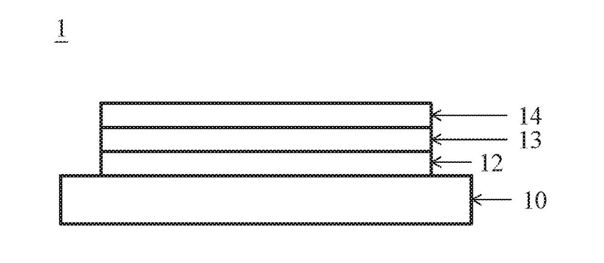
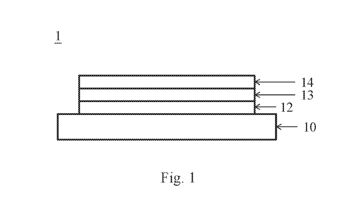
[0018]the invention discloses a substrate for a semiconductor device. The substrate comprises a ceramic supporting base plate, at least one silicon oxide layer, a first buffer layer and a gallium nitride layer. The supporting base plate is made of ceramics and formed by a polycrystalline aluminum nitride (AlN) sintered bulk body. The at least one silicon oxide layer is formed on the base plate by a sol-gel method and the silicon oxide layer has an average roughness less than the base plate to block polycrystalline orientation of the base plate and has a total thickness in a range of 10˜5000 nm. The silicon oxide layer is only formed from the sol-gel method and is not single crystalline. The first buffer layer comprises aluminum nitride (AlN) formed on the at least one silicon oxide layer with a thickness of 0.1˜10 μm and has a preferred orientation (002) AlN crystalline structure. The gallium nitride layer is formed on the first buffer layer and has a single-crystalline crystalline ...

second embodiment

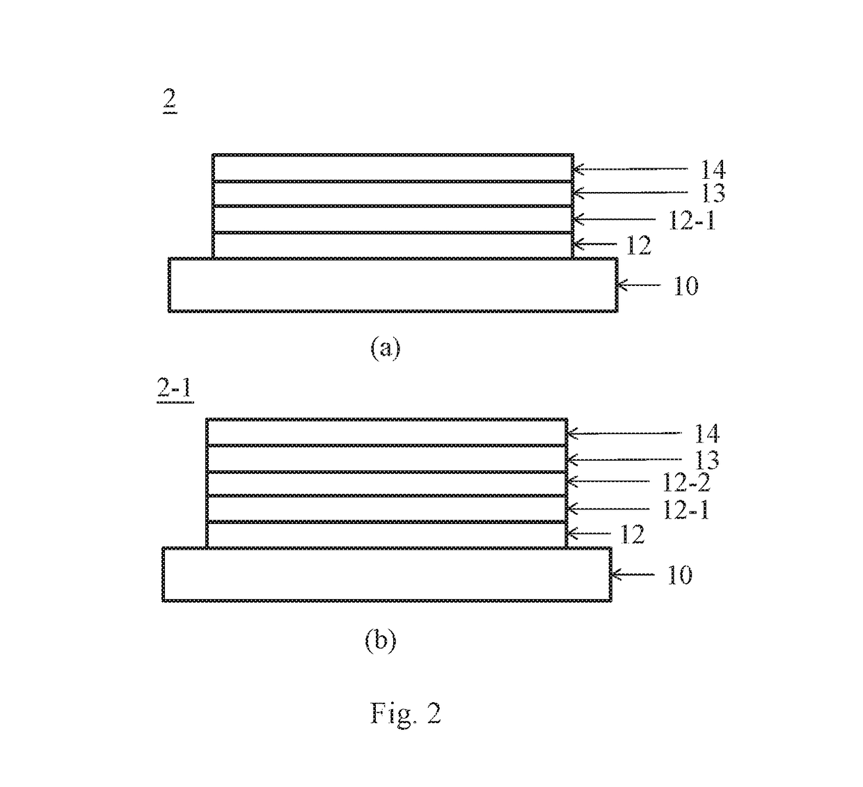
[0023]the invention discloses a method for manufacturing a substrate for a semiconductor device. The method comprises the following steps, providing a supporting base plate made of ceramics and formed by a polycrystalline aluminum nitride (AlN) sintered bulk body; performing a sol-gel process to form a silicon oxide layer at least one time wherein the sol-gel process is performed 1˜10 times, the average roughness of the top layer of the at least one silicon oxide layer is less than 25 nm and the at least one silicon oxide layer has a total thickness in a range of 10˜5000 nm; using metal-organic chemical vapor deposition to form a first buffer layer which comprises aluminum nitride (AlN) formed on the at least one silicon oxide layer; and using metal-organic chemical vapor deposition to form a gallium nitride layer formed on the first buffer layer and having a single-crystal crystalline structure. The supporting base plate is made of ceramics and formed by a polycrystalline aluminum ...


PUM


Abstract

The present invention provides a substrate for a semiconductor device and a semiconductor device using the same. The substrate for a semiconductor device comprises a ceramic supporting base plate formed by a polycrystalline aluminum nitride (AlN) sintered body; at least one silicon oxide layer formed on the base plate by a sol-gel method wherein the at least one silicon oxide layer has an average roughness less than the base plate to block polycrystalline orientation of the base plate and has a total thickness in a range of 10˜5000 nm, the silicon oxide layer is only formed from the sol-gel method and are not single crystalline; a first buffer layer comprising aluminum nitride (AlN) on the at least one silicon oxide layer with a thickness of 0.1˜10 μm; and a gallium nitride layer formed on the first buffer layer and having a single-crystal crystalline structure.

Description

BACKGROUND OF THE INVENTIONa. Field of the Invention[0001]The invention relates to a substrate for a semiconductor device and a semiconductor device using the same, particularly to a substrate containing a smooth silicon oxide layer for a semiconductor device and a semiconductor device using the same.b. Description of the Related Art[0002]Aluminum nitride is a ceramic material having electric insulation and high heat-dissipation properties because of its high thermal conductivity, crystalline structure and direct band gap properties to be extensively used as a substrate for a variety of electronic devices. A substrate is required to not only have a good heat-dissipation property but also easily grow desirable crystalline structures thereon to fabricate a semiconductor device. The heat generated in the semiconductor device has to be quickly dissipated to avoid malfunction due to overheat in the device. Particularly, a light emitting device such as high brightness light emitting diode...

Claims


Application Information

Patent Timeline
IPC IPC(8): H01L29/20H01L29/739H01L21/02H01L33/30
CPCH01L29/2003H01L33/30H01L29/7393H01L21/02389H01L21/0262H01L21/02458H01L21/0254H01L21/02491H01L21/02488H01L21/0242H01L21/02502H01L21/02505H01L29/045H01L33/0075H01L33/12H01L29/04H10N30/078
Inventor CHEN, JIANN-HENGLIN, PURUCHEN, SUN-ZEN
Owner NATIONAL CHI NAN UNIVERSITY
Why Eureka
Try Eureka