High Definition Stencils With Easy to Clean Properties for Screen Printing

a stencil and high-definition technology, applied in the field of high-definition stencil systems, can solve the problems of difficult to meet using existing technology, and achieve the effect of easy soldering or metallic, and resistance to stretching

Inactive Publication Date: 2018-01-18
PHOTO STENCIL
View PDF2 Cites 0 Cited by
  • Summary
  • Abstract
  • Description
  • Claims
  • Application Information

AI Technical Summary

Benefits of technology

[0004]The objective of this invention is to produce hard nickel and nickel-cobalt stencils (10) that are more resistant to stretching. Unique electroforming processes are developed to meet this requirement. A silicon containing amorphous carbon coating (30) is produced using the existing Dylyn amorphous carbon nanocomposite coating technology, see Patent Literature (2). On top of the Dylyn coating (30...

Problems solved by technology

These requirements are difficu...

Method used


Image

  • High Definition Stencils With Easy to Clean Properties for Screen Printing
  • High Definition Stencils With Easy to Clean Properties for Screen Printing

Examples


Embodiment Construction

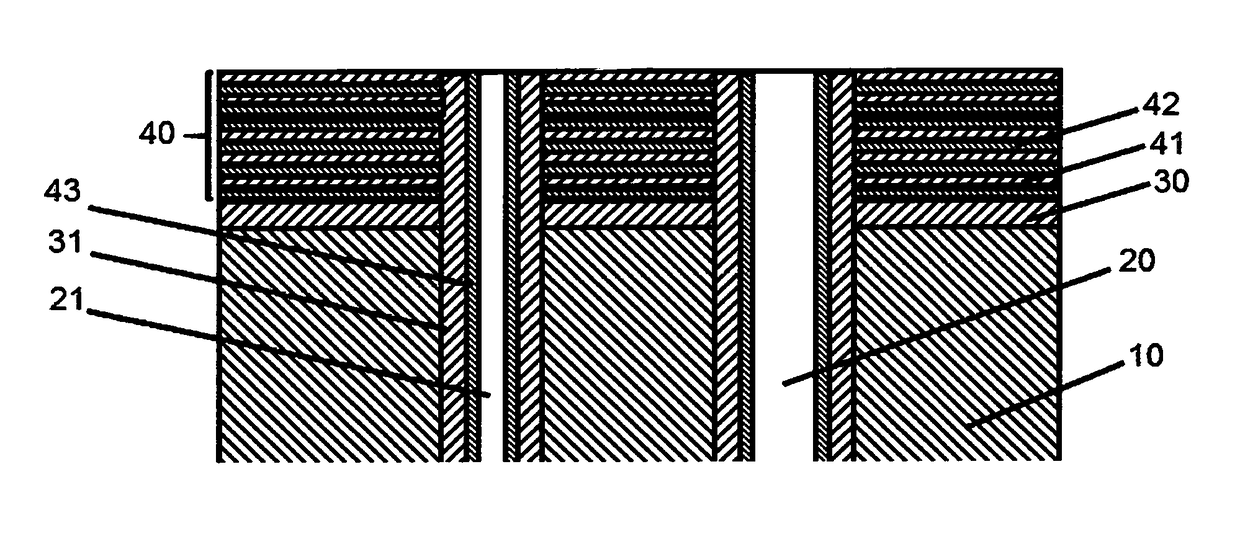
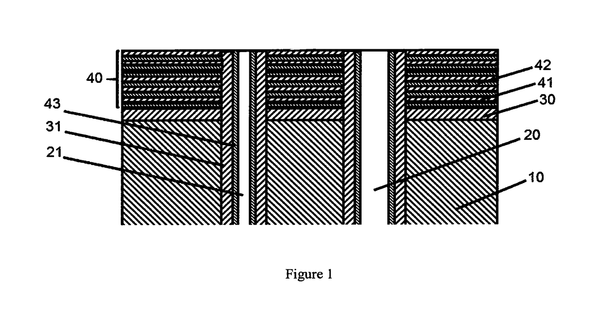
[0010]As shown in FIG. 1, the structure of the stencil is described in two embodiments as follows. In the first embodiment, the substrate stencil (10) is made of hard nickel by electroforming using a dedicated nickel-sulfamate solution. For two-dimensional stencils, the stainless steel mandrel is flat and polished to a grit 500 finish which has an average surface roughness (Ra) between 0.1 and 0.25 μm, preferably Ra is under 0.2 μm. For three-dimensional stencils, the stainless steel mandrels are polished to the same finish and then machined with pockets to enclosure the protruded chips on a PCB in designated areas. The mandrels are submerged in 25% wt to 36% wt nitric acid solution to remove residual metal debris, and then degreased by immersion in an alkaline degreaser. Subsequently, a nickel strike layer is plated on a mandrel in Woods nickel strike solution. This nickel strike solution has 220 g / l nickel chloride hexahydrate (NiCl2.6H2O) and 110 ml / l hydrochloric acid (HCl). Pur...


PUM

PropertyMeasurementUnit
Fractionaaaaaaaaaa
Thicknessaaaaaaaaaa
Thicknessaaaaaaaaaa

Abstract

This invention is for production of a screen printing stencil system with hard nickel or nickel-cobalt base metal foil (10) with amorphous carbon nanocomposite intermediate layer having low coefficient of friction (30) and alternative layers of amorphous carbon nanocomposite (41) and amorphous fluorocarbon (42) optimized for its wettability in broad contact areas between squeegee blade and the stencil and oleophobic amorphous fluorocarbon-rich coatings (43) on the inner walls of through holes (20) and (21) to provide easy release of solder paste or metallic paste for high definition screen plating of small feature dimensions and easy to clean properties.

US Patent Documents
(1) 20130220152
Febuary 2013
K. Shibusawa
(2) 6228471 B1
May 2001
Neerinck et al

Description

FIELD OF APPLICATION[0001]This invention is about to produce a screen printing stencil system with layered structures of amorphous carbon nanocomposite and amorphous fluorocarbon coatings for high dimensional definition and easy to clean properties.BACKGROUND OF THE INVENTION[0002]As the feature dimensions of printed circuit boards (PCB) become smaller, it would be most desirable to produce these features with stencils which apply solder or metallic paste with high definition without bleeding out the paste and high positional accuracy without stretching. Current stainless steel and pure nickel stencils are too ductile to meet such requirements because they are more vulnerable to stretching and deformation. They also tend to trap and bleed residual paste without oleophobicity. In particular, the paste with high viscosity is more difficult to produce smooth plate separation for high definition applications. Patent literature (1) discloses a method of manufacturing stencils with layere...

Claims


Application Information

Patent Timeline
IPC IPC(8): B41N1/24C23C14/00
CPCC23C14/00B41N1/24C23C14/06C23C16/30C23C16/45523H05K3/1225B41C1/142
Inventor CHEN, GUOCUN
Owner PHOTO STENCIL
Why Eureka
Try Eureka