Sample observation method and sample observation device

a sample observation and sample technology, applied in image enhancement, instruments, caliper-like sensors, etc., can solve the problem of the resolution limit of an acquired image of approximately several hundred nanometers, and achieve the effect of reducing burden and burden

Active Publication Date: 2018-01-18
HITACHI HIGH-TECH CORP
View PDF2 Cites 16 Cited by
  • Summary
  • Abstract
  • Description
  • Claims
  • Application Information

AI Technical Summary

Benefits of technology

[0020]According to the present invention, a defect observation device including a plurality of detectors can output an image from which a defect and a circuit pattern are highly visible, thereby enabling a user to reduce the burden when the user carries out image viewing work.
[0021]In addition, according to the present invention, in view of visibility of a defect site or a circuit pattern from a plurality of images detected by a plurality of detectors, a mixed image can be generated by automatically adjusting and mixing weighting factors required when the plurality of images are mixed (synthesized) with each other, thereby enabling the user to reduce the burden when the user carries out the image viewing work. The problems, configurations, and advantageous effects other than those described above will be clarified by the description of the following embodiments.

Problems solved by technology

However, according to this optical inspection device, a resolution limit of an acquired image is approximately several hundred nanometers due to the influence of the illumination wavelength.

Method used


Image

  • Sample observation method and sample observation device
  • Sample observation method and sample observation device
  • Sample observation method and sample observation device

Examples


embodiment 1

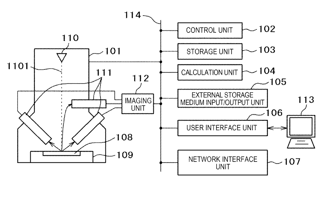
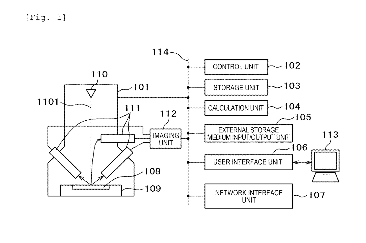
[0047]Hereinafter, a defect observation device according to the present invention will be described. In the present embodiment, an observation device including a scanning electron microscope (SEM) will be described as a target. However, an imaging device according to the present invention may be a device other than SEM, and may be an imaging device using a charged particle such as ion.

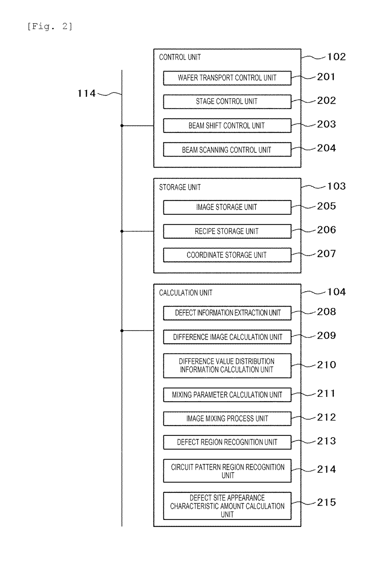
[0048]FIG. 1 illustrates an overall configuration of the device according to the present invention. The device includes SEM 101 for capturing an image, a control unit 102 for performing overall control, a storage unit 103 for storing information in a magnetic disk or a semiconductor memory, a calculation unit 104 for performing calculation in accordance with a program, an external storage medium input / output unit 105 for inputting and outputting information to and from an external storage medium connected to the device, a user interface unit 106 for controlling the input / output of user's information, a...

embodiment 2

[0088]In Embodiment 1, a method for outputting the highly visible image of various defects has been described. In Embodiment 2, a method for generating and outputting a highly visible image of not only the defect but also the circuit pattern will described.

[0089]A device configuration according to the present embodiment is the same as that illustrated in FIGS. 1 and 2 in Embodiment 1. In addition, a main flow of the observation process is also the same as the flow of the observation process described with reference to FIG. 6. A different point is a processing method of the mixed image generation process (S606). Hereinafter, only elements different from those in Embodiment 1 will be described.

[0090]In the image mixing method according to the present embodiment, the detector image is discriminated into a defect region and a region other than the defect (background region), the mixing parameter is calculated for each region, and the images are mixed using the mixing parameters which ar...

embodiment 3

[0098]In Embodiment 1 and Embodiment 2, a method has been described in which the mixing parameter is calculated using the detector image so as to mix the highly visible image of the defect site and the circuit pattern. In the present embodiment, a method will be described in which a highly visible observation image is obtained for ADR.

[0099]ADR is a function to automatically collect observation images, based on defect position coordinates output by another defect inspection device. The defect position coordinates output by the inspection device include an error. Accordingly, ADR is provided with a function to re-detect the defect from an image obtained by imaging the defect position coordinates with low magnification, and to mainly image the re-detected defect position as a high magnification image for observation. In the present embodiment, a method will be described in which the mixing parameter is calculated from a low magnification image so as to be used in mixing the images for...


PUM


Abstract

An inspection method uses a charged particle microscope to observe a sample and view a defect site or a circuit pattern. A plurality of images is detected by a plurality of detectors and a mixed image is generated by automatically adjusting and mixing weighting factors required when the plurality of images are synthesized with each other. The sample is irradiated and scanned with a charged particle beam so that the plurality of detectors arranged at different positions from the sample detects a secondary electron or a reflected electron generated from the sample. The mixed image is generated by mixing the plurality of images of the sample with each other for each of the plurality of detectors, which are obtained by causing each of the plurality of detectors arranged at the different positions to detect the secondary electron or the reflected electron. The generated mixed image is displayed on a screen.

Description

TECHNICAL FIELD[0001]The present invention relates to a method and a device for observing a defect or a circuit pattern appearing while semiconductor wafers are manufactured, and more particularly relates to a device provided with a method and means for outputting an image from which the defect or the circuit pattern is highly visible by using an image obtained from a plurality of detectors included in a charged particle microscope.BACKGROUND ART[0002]When the semiconductor wafers are manufactured, it is important to quickly start a manufacturing process and to shift to a high-yield mass-production system at an early stage in order to ensure profitability. For this purpose, various inspection / measurement devices are introduced to manufacturing lines.[0003]As a representative inspection device, an optical wafer inspection device is known. For example, JP-A-2000-105203 (PTL 1) discloses a technique for inspecting the defect in such a way that an optical image of a wafer surface is cap...

Claims


Application Information

Patent Timeline
Patent Type & Authority Applications(United States)
IPC IPC(8): H01J37/22G06T5/50G01B15/04G06T7/00
CPCH01J37/22G01B15/04G06T5/50G06T7/001G06T2207/10061G06T2207/30148G01N23/22G01B2210/48H01J37/244H01J37/28H01J2237/24465H01J2237/24495H01J2237/24585
Inventor HARADA, MINORUTAKAGI, YUJIHIRAI, TAKEHIRO
Owner HITACHI HIGH-TECH CORP
Why Eureka
Try Eureka