Interference-free fingerprint identification device

a fingerprint identification and interference-free technology, applied in the field of fingerprint identification, can solve the problems of reducing the sensitivity of fingerprint identification, reducing the signal size, and affecting the accuracy of fingerprint identification, so as to reduce the chip area, reduce the cost, and simplify the package

Active Publication Date: 2018-01-25
SUPERC TOUCH CORP
View PDF0 Cites 14 Cited by
  • Summary
  • Abstract
  • Description
  • Claims
  • Application Information

AI Technical Summary

Benefits of technology

[0005]The object of the present invention is to provide an interference-free fingerprint identification device, which has the advantages of low cost and simple package. In the interference-free fingerprint identification device, thin film transistors are used to form a thin film transistor layer on a substrate, wherein the thin film transistor layer is disposed on one side of the substrate and includes plural thin film transistors. A sensing electrode layer is provided with plural fingerprint sensing electrodes, each corresponding to at least three thin film transistors, and the sensing electrode is connected to the sources or drains of the corresponding thin film transistors. A gate line layer is provided with plural gate lines. A data line layer is provided with plural data lines. A first shielding layer is disposed between the gate line layer and the data line layer, and is electrically connected to a source or drain of a thin film transistor in a plurality of the thin film transistors. The interference-free fingerprint identification device is further provided with a fingerprint identification integrated circuit chip which is electrically connected to the thin film transistor substrate. Accordingly, it not only reduces chip area and simplifies the package process, but also easily increases the sensing area and facilitates the realization of curved surface sensing. Moreover, it can also enhance the accuracy of biometrics, significantly improve the manufacturing yield, and greatly reduce the manufacturing cost.

Problems solved by technology

However, due to that the sensing signal is extremely small and the surrounding noise is huge and complicated, the sensing electrodes and the sensing circuit are packaged in one integrated circuit (IC) chip for the press type fingerprint identification.
To prevent the lead lines of the fingerprint identification IC chip package from damage, epoxy resin is applied to protect the lead lines, resulting in adding a distance with several tens of micrometers (μm) between the sensing electrodes and the finger, which dramatically reduces the sensitivity of the fingerprint identification.
In addition, due to addition of this distance with several tens of micrometers (μm), it also increases the difficulty of product integration.
However, this is not only increasing the material cost and the package process cost, but also decreasing the product yield and the product lifetime and reliability.

Method used


Image

  • Interference-free fingerprint identification device
  • Interference-free fingerprint identification device
  • Interference-free fingerprint identification device

Examples


first embodiment

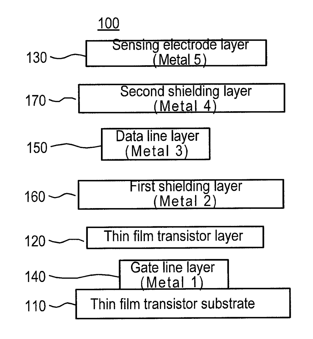
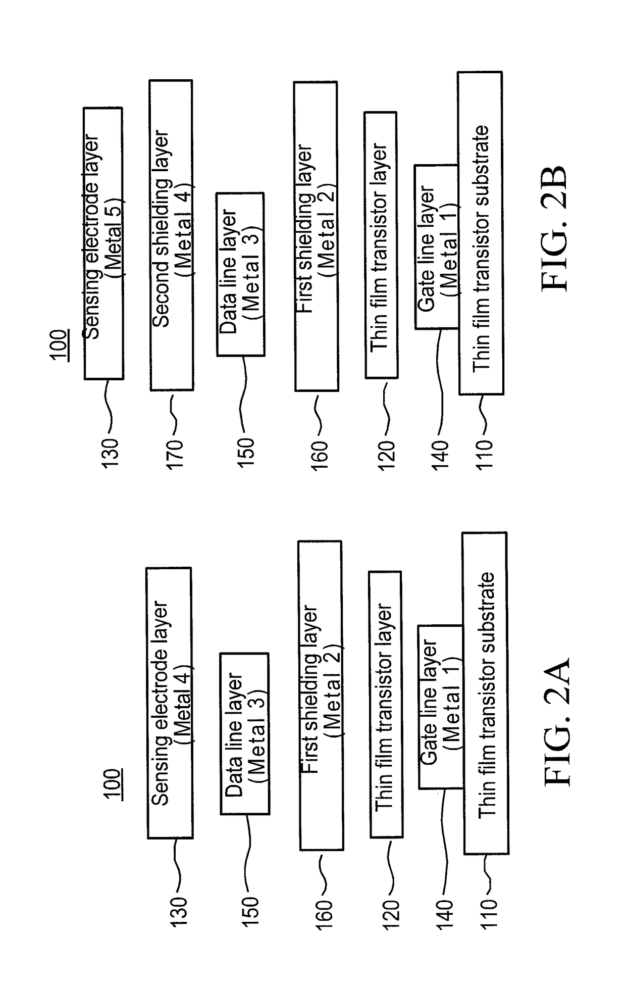
[0034]FIG. 3A and FIG. 3B are another cross-sectional views of the interference-free fingerprint identification device in accordance with the present disclosure, wherein the insulation layers between the conductive layers are represented by spaces and are not specifically indicated. In comparison with FIG. 2A and FIG. 2B, FIG. 3A and FIG. 3B are each additionally provided with a black matrix layer (BM) 180. The black matrix layer 180 may be black color and disposed between the thin film transistor substrate 110 and the sensing electrode layer 130. The difference between FIGS. 3A and 3B and FIGS. 2A and 2B is that the thin film transistor substrate 110 is located at top in FIG. 3A and FIG. 3B. That is, in FIG. 3A and FIG. 3B, the thin film transistor substrate 110 may serve as a protective layer of the plural fingerprint sensing electrodes 131 in the sensing electrode layer 130 when the thin film transistor substrate 110 is made of a glass material having a sufficient hardness. The t...

second embodiment

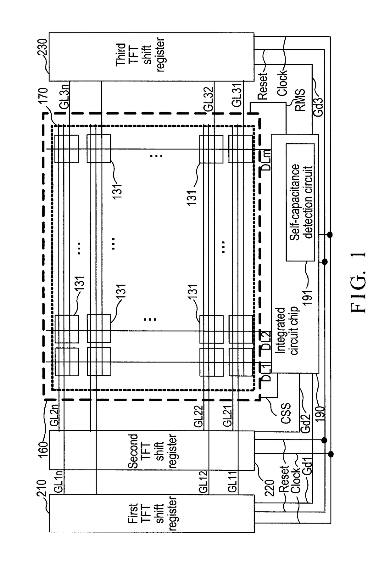
[0052]FIG. 13 is a schematic diagram of an interference-free fingerprint identification device in accordance with the present disclosure. This embodiment is similar to that of FIG. 1 except that the second shielding layer 170 is removed in FIG. 13. Plural common data lines CDL1, CDL2, . . . , CDLn are arranged in the gate line layer 140, which are parallel with the gate lines GL11, GL12, . . . , GL1n, GL21, GL22, . . . , GL2n, GL31, GL32, . . . , GL3n. The common data line CDL1 is electrically connected to the sources or drains of a plurality of the thin film transistors corresponding to the fingerprint sensing electrodes 131 of the first row, the common data line CDL2 is electrically connected to the sources or drains of a plurality of the thin film transistors corresponding to the finger sensing electrodes 131 of the second row, and so on. The plural common data lines CDL1, CDL2, CDLn are electrically connected together, and the integrated circuit chip 190 outputs a convergence st...

third embodiment

[0053]FIG. 14 is a schematic diagram of an interference-free fingerprint identification device 100 in accordance with the present disclosure. This embodiment is similar to that of FIG. 13 except that the first TFT shift register 210, the second TFT shift register 220 and the third TFT shift register 230 are removed in FIG. 14. The integrated circuit chip 190 directly outputs a control signal to the gate lines GL11, GL12, GL1n, GL21, GL22, GL2n, GL31, GL32, GL3n, CDL1, CDL2, . . . , CDLn through a gate line bus GLBus. Plural common data lines CDL1, CDL2, CDLn are disposed in the gate line layer 140. The common data line CDL1 is electrically connected to the sources or drains of a plurality of the thin film transistors corresponding to the fingerprint sensing electrodes 131 of the first row, the common data line CDL2 is electrically connected to the sources or drains of a plurality of the thin film transistors corresponding to the finger sensing electrodes 131 of the second row, and s...


PUM


Abstract

An interference-free fingerprint identification device includes a TFT substrate, a TFT layer having plural TFTs, a sensing electrode layer having plural fingerprint sensing electrodes, a gate line layer having plural gate lines, a data line layer having plural data lines, and a first shielding layer. Each fingerprint sensing electrode corresponds to a plurality of the TFTs, and is connected to sources or drains of at least two corresponding TFTs. At least two gate lines are electrically connected to gates of a plurality of the TFTs corresponding to a fingerprint sensing electrode. Each data line is electrically connected to a source or drain of a TFT in a plurality of the TFTs corresponding to a fingerprint sensing electrode. The first shielding layer is electrically connected to a source or drain of a TFT in a plurality of the TFTs corresponding to each fingerprint sensing electrode.

Description

BACKGROUND OF THE INVENTION1. Field of the Invention[0001]The present invention relates to the technical field of fingerprint identification and, more particularly, to an interference-free fingerprint identification device.2. Description of Related Art[0002]Due to the rising of e-commerce, the development of remote payment is dramatically increasing, so that the business demands for the biometrics are also rapidly expanded. The biometrics technology can be divided into the fingerprint identification technology, the iris identification technology, the DNA identification technology, and so on. In order to satisfy the requirements of efficiency, safety, and non-invasiveness, the fingerprint identification technology has become the preferred technology for the biometrics technology. The fingerprint identification technology can be divided into the optical identification, the thermal induction identification, the ultrasonic identification, and the capacitive identification. In considerat...

Claims


Application Information

Patent Timeline
Patent Type & Authority Applications(United States)
IPC IPC(8): G06K9/00G06F3/044H01L27/146G07C9/00G06F3/041H01L27/12G06V40/13
CPCG06K9/00013G06F3/0418G06F3/044H01L27/14678G07C9/00158H01L27/1214H01L29/78633G06F3/0443G06F3/0446G06V40/13G07C9/37
Inventor LEE, HSIANG-YUCHIN, SHANGLIN, PING-TSUN
Owner SUPERC TOUCH CORP
Why Eureka
Try Eureka