Trench Edge Termination Structure for Power Semiconductor Devices

a technology of power semiconductor devices and termination structures, which is applied in the direction of semiconductor devices, basic electric elements, electrical equipment, etc., can solve the problems of high cost, large occupied area, and no square chip application of either of them

Inactive Publication Date: 2018-01-25
UNIV OF ELECTRONICS SCI & TECH OF CHINA +1
View PDF3 Cites 8 Cited by
  • Summary
  • Abstract
  • Description
  • Claims
  • Application Information

AI Technical Summary

Benefits of technology

[0010]Some beneficial effects of the present invention are as follow. On one hand, compared with fabricating a trapezoidal or rectangle trench, fabricating a trench with a sectional shape of inverted trapezium by deep trench etching and dielectric filling is less difficult. On the other hand, due to the Coulomb interaction between the ionized impurity in the drift region and the fixed charges introduced at a particular location in the trench, the depletion region of the terminal PN junction can be fully extended such that the concentration of electric field, is relieved. Therefore, the edge termination provided in this invention can exhibit a high breakdown voltage which approaches the high breakdown voltage of the parallel plane junction with a smaller area.

Problems solved by technology

Therefore, in high voltage devices, the large extended terminal structures result in the rise of the cost.
Neither of them is applicable to the square chip, and their occupied areas are very large, especially the negative grinding angle technology.
The advantage of this kind of trench termination is that the occupied area is small, while the disadvantages are that the deep trench process is more complex, and the breakdown is affected by the trench wall morphology, trench filling material, and other factors.
However, the process to fabricate such a regular trapezoid trench and fill it well is difficult.
However, this scheme needs a very large area.

Method used


Image

  • Trench Edge Termination Structure for Power Semiconductor Devices
  • Trench Edge Termination Structure for Power Semiconductor Devices
  • Trench Edge Termination Structure for Power Semiconductor Devices

Examples


embodiment 1

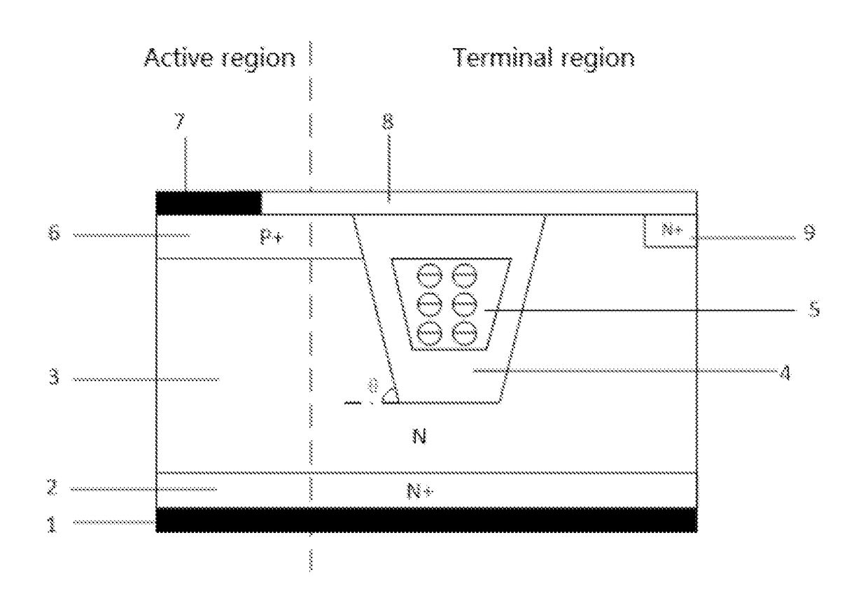
[0019]FIG. 1 illustrates a trench edge termination of power semiconductor device in accordance with the present invention. The edge termination structure includes: a P-type heavily doped substrate 2, a P-type lightly doped drift region 3 located on the top surface of the P-type heavily doped substrate 2. a drain electrode 1 located on the lower surface of the P-type heavily doped substrate 2, and a field oxide 8 on the upper surface of the P-type lightly doped drift region 3. The P-type lightly doped drift region 3 includes a trench 4 and a P-type heavily doped region 9. The P-type heavily doped region 9 is located in the top portion of the P-type lightly doped drill region 3 and on the side away from the device active region, and the upper surface of the P-type heavily doped region 9 contacts the lower surface of the field oxide 8. The trench 4 is filled with an insulating material and its upper surface contacts the lower surface of the field oxide 8. In trench 4, there is a polysi...

embodiment 2

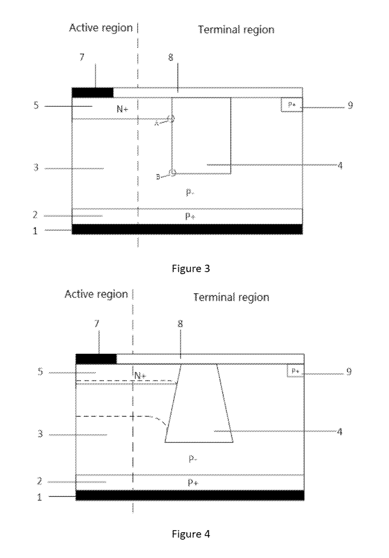
[0037]FIG. 16 shows a further embodiment. In this embodiment, on the basis of embodiment 1, all the N-type materials are replaced by P-type materials, and all P-type materials are replaced by N-type materials, and the fixed positive charge in the floating island 5 is replaced by fixed negative charge.

[0038]In addition, in both embodiment 1 and embodiment 2. some other semiconductor materials such as silicon, carbide, gallium arsenide, indium phosphide and germanium silicon can be used to replace silicon in manufacturing.


PUM


Abstract

Edge termination structures for power semiconductor devices (or power devices) are disclosed. The purpose of this invention is to reduce the difficulty of deep trench etching and dielectric filling by adopting an inverted trapezoidal trench. In order to save the area of edge termination and get a high blocking voltage on condition that the angle between the sidewall of the trench and horizontal is large, fixed charges are introduced at a particular location in the trench. Due to the Coulomb interaction between the ionized impurity in the drift region and the fixed charges, the depletion region of the terminal PN junction can extend fully, which relieves the concentration of electric field there. Therefore, the edge termination can exhibit a high breakdown voltage near to that of the parallel plane junction with a smaller area and the reduced technical difficulty of deep trench etching and dielectric filling.

Description

CROSS REFERENCE[0001]The present application is based on, and claims priority from, Chinese application number 201610587297.5, filed on Jul. 25, 2016, the disclosure of which is hereby incorporated by reference herein in its entirety.TECHNICAL FIELD OF THE INVENTION[0002]This invention generally, relates to the field of semiconductor technology, and more particularly to trench edge termination structures for power semiconductor devices.BACKGROUND OF THE INVENTION[0003]The blocking voltage of a power device depends mainly on the reverse bias breakdown voltage of particular PN junction in the devices. Influenced by the non-ideal factors at the termination of PN junction, the reverse breakdown voltage of an actual PN junction is much lower than the parallel plane junction. Junction termination is a specifically designed structure to reduce the local electric field intensity improve the reliability and enhance the breakdown voltage of an actual PN junction close to the parallel plane ju...

Claims


Application Information

Patent Timeline
Patent Type & Authority Applications(United States)
IPC IPC(8): H01L29/78H01L21/306H01L29/40H01L29/06H01L29/10H01L29/417
CPCH01L29/7811H01L29/1079H01L29/1095H01L29/41741H01L29/405H01L29/0649H01L29/0611H01L29/0684H01L29/0661H01L21/30604H01L29/0657H01L29/0692H01L29/407H01L29/0638
Inventor REN, MINXIE, CHILI, JIAJUZHONG, ZIQILI, ZEHONGZHANG, JINPINGGAO, WEIZHANG, BO
Owner UNIV OF ELECTRONICS SCI & TECH OF CHINA
Why Eureka
Try Eureka