Method for manufacturing quantum dot color filter substrate

a color filter substrate and quantum dot technology, applied in the field of display technology, can solve the problems of affecting the performance of the qds, wasting large quantities of quantum dot materials, and difficult to develop photoresist materials with high light emission efficiency, etc., and achieves the effects of simple operation, short time period, and high light emission efficiency

Active Publication Date: 2018-02-01
TCL CHINA STAR OPTOELECTRONICS TECH CO LTD
View PDF3 Cites 28 Cited by
  • Summary
  • Abstract
  • Description
  • Claims
  • Application Information

AI Technical Summary

Benefits of technology

[0007]An object of the present invention is to provide a method for manufacturing a quantum dot color filter substrate, which uses a grey level patterns formed on a photo mask to form, through one process of exposure and development, pixel barrier walls, main spacers, and sub spacers, and then forms patterned quantum dot layers in zones delimited and surrounded by the pixel barrier walls through inkjet printing and which has a simple operation, takes a short period of time, has a reduced expenditure of facility installation, and shows high utilization of quantum dot materials.
[0015](5) subjecting the black barrier walls, the transparent barrier walls, the sub spacers, and the main spacers to baking in order to remove a major portion of solvent contained therein and improve curing degree and attaching capability; and
[0037](5) subjecting the black barrier walls, the transparent barrier walls, the sub spacers, and the main spacers to baking in order to remove a major portion of solvent contained therein and improve curing degree and attaching capability; and
[0042]A beneficial effect of the present invention is that the present invention provides a method for manufacturing a quantum dot color filter substrate, in which a black photoresist layer and a transparent photoresist layer are first coated and formed on a backing plate in sequence and then, first, second, and third patterns of a photo mask having different grey levels are used to pattern the black photoresist layer and the transparent photoresist layer to obtain a plurality of transparent barrier walls corresponding to the first pattern, sub spacers corresponding to the second pattern and located on the transparent barrier walls, and main spacers corresponding to the third pattern and located on the transparent barrier walls and also to obtain a plurality of black barrier walls covered by the plurality of transparent barrier walls, the plurality of black barrier walls and the plurality of transparent barrier walls located thereon collectively defining a plurality of pixel barrier walls; and then, patterned quantum dot layers are formed in sub-pixel zones that are delimited and surrounded by the plurality of pixel barrier walls by means of inkjet printing such that accuracy of inkjet printing is greatly improved. The method for manufacturing a quantum dot color filter substrate has a simple operation, takes a short period of time, has a reduced expenditure of facility installation, and shows high utilization of quantum dot materials.

Problems solved by technology

When QDs are dispersed in the photoresist, due to the QDs being nanometer particles, they may very easily react with the initiator so as to abruptly lower down light emission efficiency or even get quenching thereby affecting the performance of the QDs.
Thus, development of photoresist materials having high light emission efficiencies is difficult.
Further, the development process of photolithography may remove unnecessary portions through development so as to lead to a great waste of the quantum dot material.

Method used


Image

  • Method for manufacturing quantum dot color filter substrate
  • Method for manufacturing quantum dot color filter substrate
  • Method for manufacturing quantum dot color filter substrate

Examples


Embodiment Construction

[0052]To further expound the technical solution adopted in the present invention and the advantages thereof, a detailed description is given to a preferred embodiment of the present invention and the attached drawings.

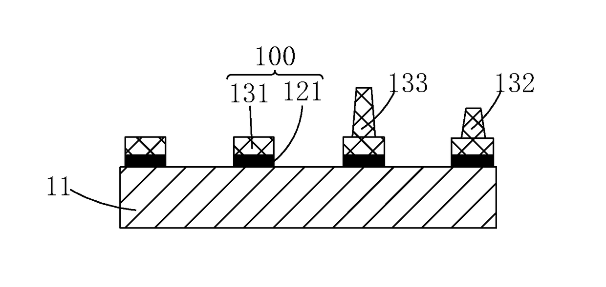
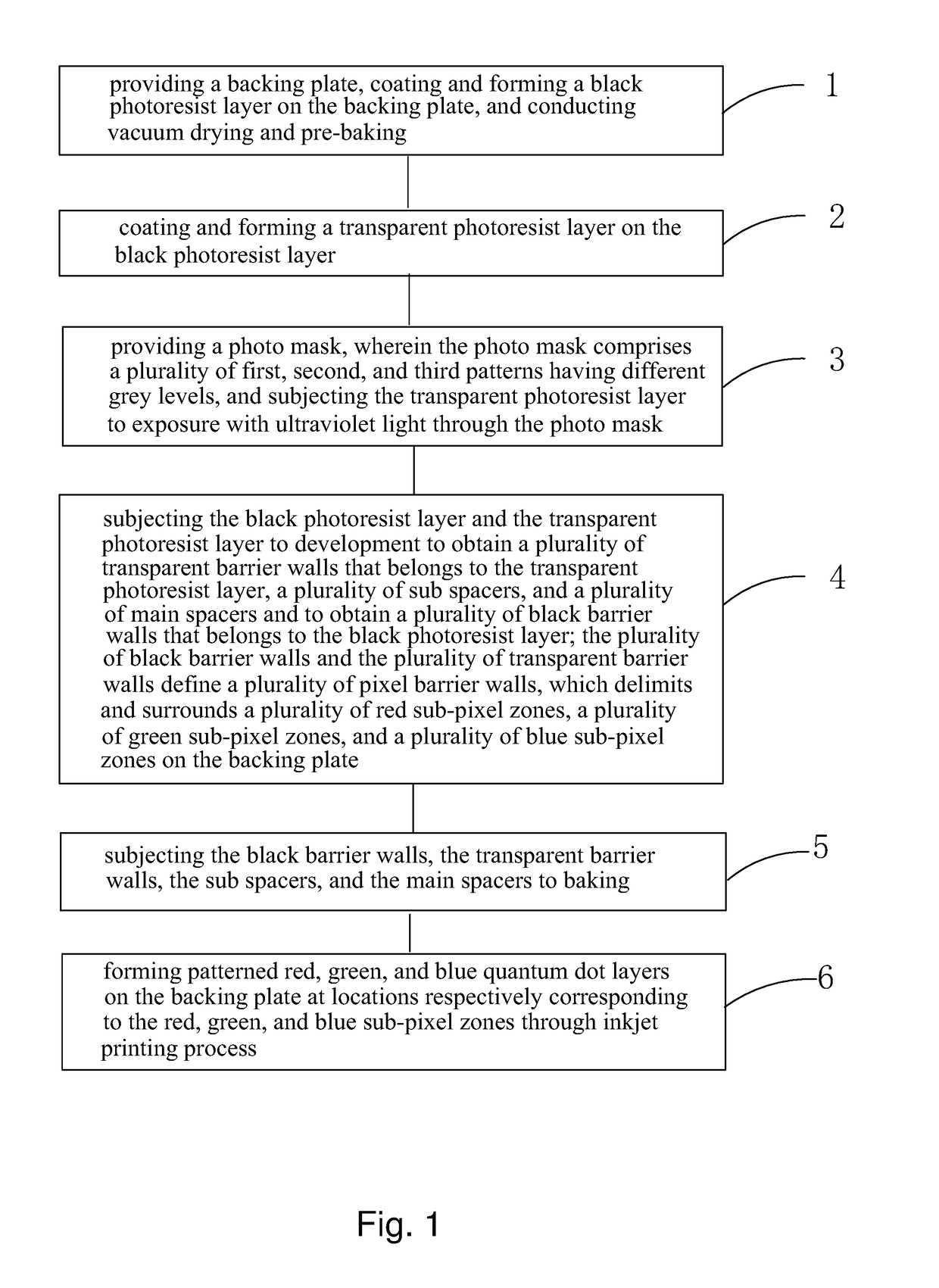
[0053]Referring to FIG. 1, firstly, the present invention provides a method for manufacturing a quantum dot color filter substrate, which comprises the following steps:

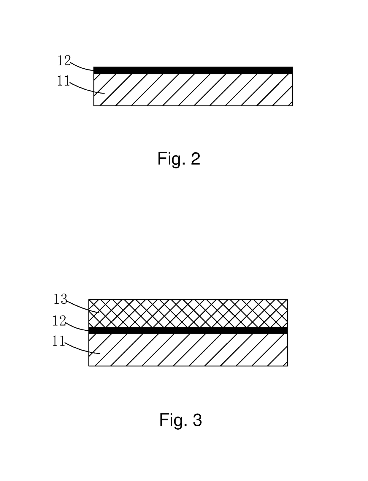
[0054]Step 1: as shown in FIG. 2, providing a backing plate 11, coating and forming a black photoresist layer 12 on the backing plate 11, and subjecting the black photoresist layer 12 to vacuum drying and pre-baking in order to remove a portion of solvent contained in the black photoresist layer 12.

[0055]Specifically, the black photoresist layer 12 is formed by means of slit coating or spin coating and the black photoresist layer 12 has a thickness of 0.5-2 μm.

[0056]Step 2: as shown in FIG. 3, coating and forming a transparent photoresist layer 13 on the black photoresist layer 12.

[0057]Specifically, the...


PUM

PropertyMeasurementUnit
thicknessaaaaaaaaaa
thicknessaaaaaaaaaa
particle sizeaaaaaaaaaa

Abstract

The present invention provides a method for manufacturing a quantum dot color filter substrate, in which a black photoresist layer and a transparent photoresist layer are first coated and formed on a backing plate in sequence and then, first, second, and third patterns of a photo mask having different grey levels are used to pattern the black photoresist layer and the transparent photoresist layer to obtain a plurality of transparent barrier walls corresponding to the first pattern, sub spacers corresponding to the second pattern and located on the transparent barrier walls, and main spacers corresponding to the third pattern and located on the transparent barrier walls and also to obtain a plurality of black barrier walls covered by the plurality of transparent barrier walls, the plurality of black barrier walls and the plurality of transparent barrier walls located thereon collectively defining a plurality of pixel barrier walls; and then, patterned quantum dot layers are formed in sub-pixel zones that are delimited and surrounded by the plurality of pixel barrier walls by means of inkjet printing such that accuracy of inkjet printing is greatly improved.

Description

BACKGROUND OF THE INVENTION1. Field of the Invention[0001]The present invention relates to the field of display technology, and in particular to a method for manufacturing a quantum dot color filter substrate.2. The Related Arts[0002]Due to various advantages, such as high colorfulness, compactness, and low power consumption, thin-film transistor liquid crystal displays (TFT-LCDs) are now taking a leading position in the field of flat panel displays. A color filter, which is one of the important components of a liquid crystal display, generally achieves color displaying by means of color resist layers of red (R), green (G), and blue (B).[0003]With the continuous development of the display technology, people increasingly demand higher and higher quality of displaying. Quantum dots (QDs) are semiconductor particles having a particle size of 1-100 nm. Since the particle size of QDs is relatively small, less than or close to the exciton Bohr radius of the corresponding body material, an...

Claims


Application Information

Patent Timeline
Patent Type & Authority Applications(United States)
IPC IPC(8): G02F1/1335G02F1/1368B05D1/00G02F1/1339
CPCG02F1/133516G02F1/13394G02F1/133512G02F1/133617G02F1/1368G02F1/133528B05D1/005G02F2001/13396G02F2001/133614G02F2202/36G02F1/133514G02F1/133614B82Y20/00B82Y40/00G02F1/13396G02F1/1335
Inventor LI, LANYANLIANG, YUHENG
Owner TCL CHINA STAR OPTOELECTRONICS TECH CO LTD
Why Eureka
Try Eureka