Printable 3D electronic structure

Active Publication Date: 2018-02-08
X DISPLAY CO TECH LTD
View PDF5 Cites 23 Cited by
  • Summary
  • Abstract
  • Description
  • Claims
  • Application Information

AI Technical Summary

Benefits of technology

[0027]In some embodiments of the present invention, two or more directly electrically connected connection posts are provided to contact a common destination substrate contact pad. In some embodiments, two or more directly electrically connected contact pads are provided to contact one or more directly electrically connected connection posts. By providing two or more connection posts in contact with a common destination substrate contact pad or providing two or more component contact pads in contact with a commonly electrically connected connection posts, faults in electrical connections between the component and the destination substrate

Problems solved by technology

The above techniques have some limitations.
Despite processing methods used to improve the performance of thin-film transistors, such transistors may provide performance that is lower than the performance of other integrated circuits formed in mono-crystalline semiconductor material.
Semiconductor material and active components can be provided only on portions of the substrate, leading to wasted material and increased material and processing costs.
The choice of substrate materials can also be limited by the processing steps necessary to process the semiconductor material and the photo-lithographic steps used to pattern the active components.
For example, plastic substrates have a limited chemical and heat tolerance and do not readily survive photo-lithographic processing.
Furthermore, the manufacturing equipment used to process large substrates with thin-film circuitry is relatively expensive.
However, such substrate materials can be more expensive or difficult to process.
However, these techniques may be limited in the size of the integrated circuits that can be placed.
While this approach can provide substrates with the same performance as integrated circuits, the size of such substrates may be limited, for example, to a 12-inch diameter circle, and the wafers are relatively expensive compared to other substrate materials such as glass, polymer, or quartz.
However, the bonding technique and the processing equipment for the substrates to form the thin-film active components on large substrates can be relatively expensive.
This method may require etching a significant quantity of ma

Method used


Image

  • Printable 3D electronic structure
  • Printable 3D electronic structure
  • Printable 3D electronic structure

Examples


Embodiment Construction

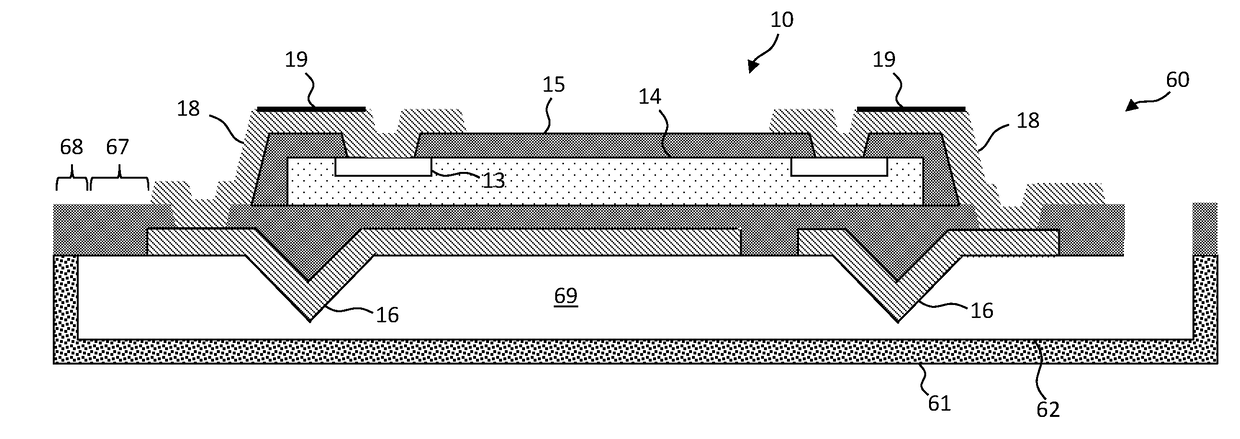
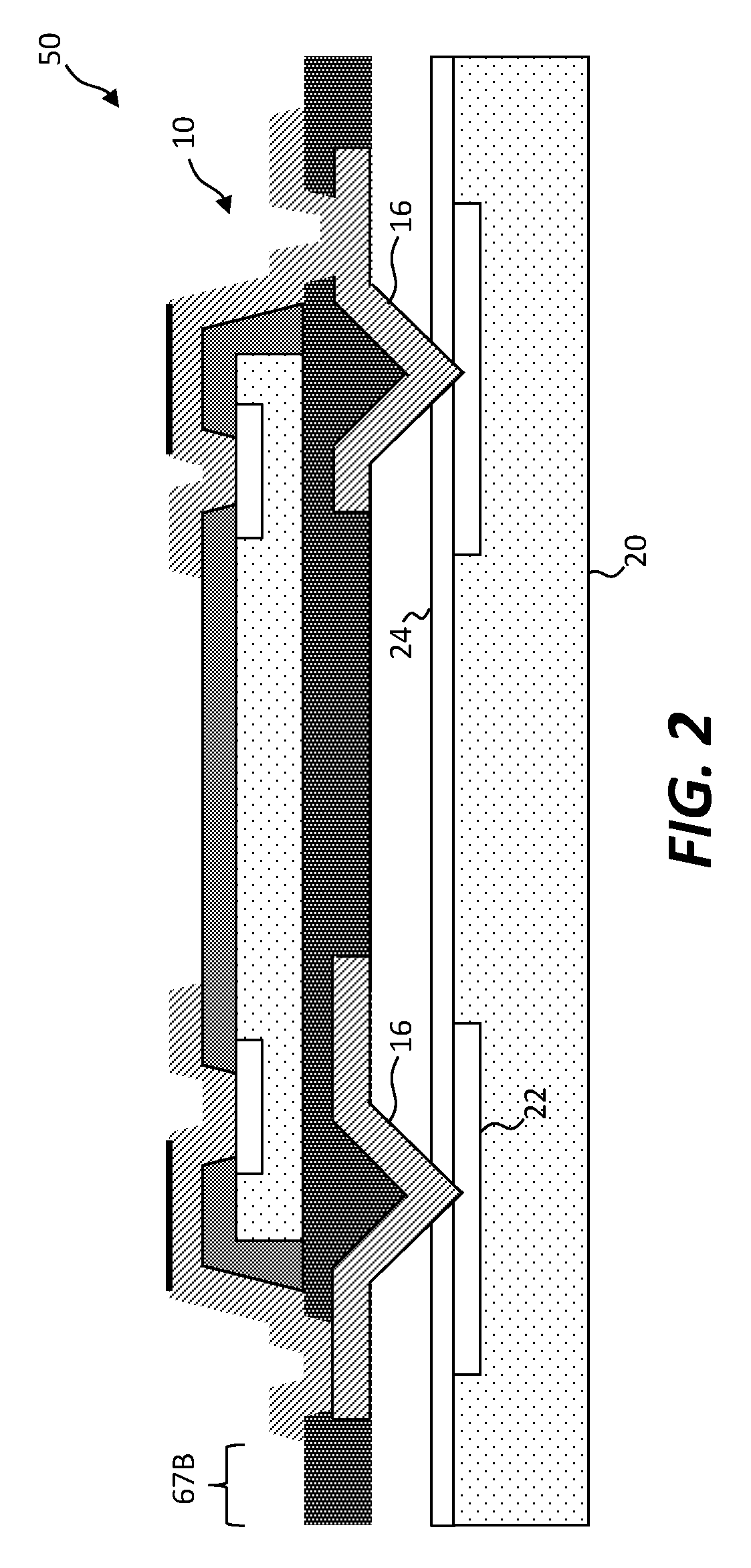
[0049]The present invention provides, inter alia, structures and methods for electrically connecting relatively small electrical components such as integrated circuit chiplets in a simple, efficient, extensible, flexible, and cost-effective way. The integrated circuit chiplets (chiplets) can be electrically connected to a destination substrate or one chiplet can be electrically connected directly to another chiplet, for example in a three-dimensional stack of chiplets, or to three or more chiplets, forming a three-dimensional electronic structure.

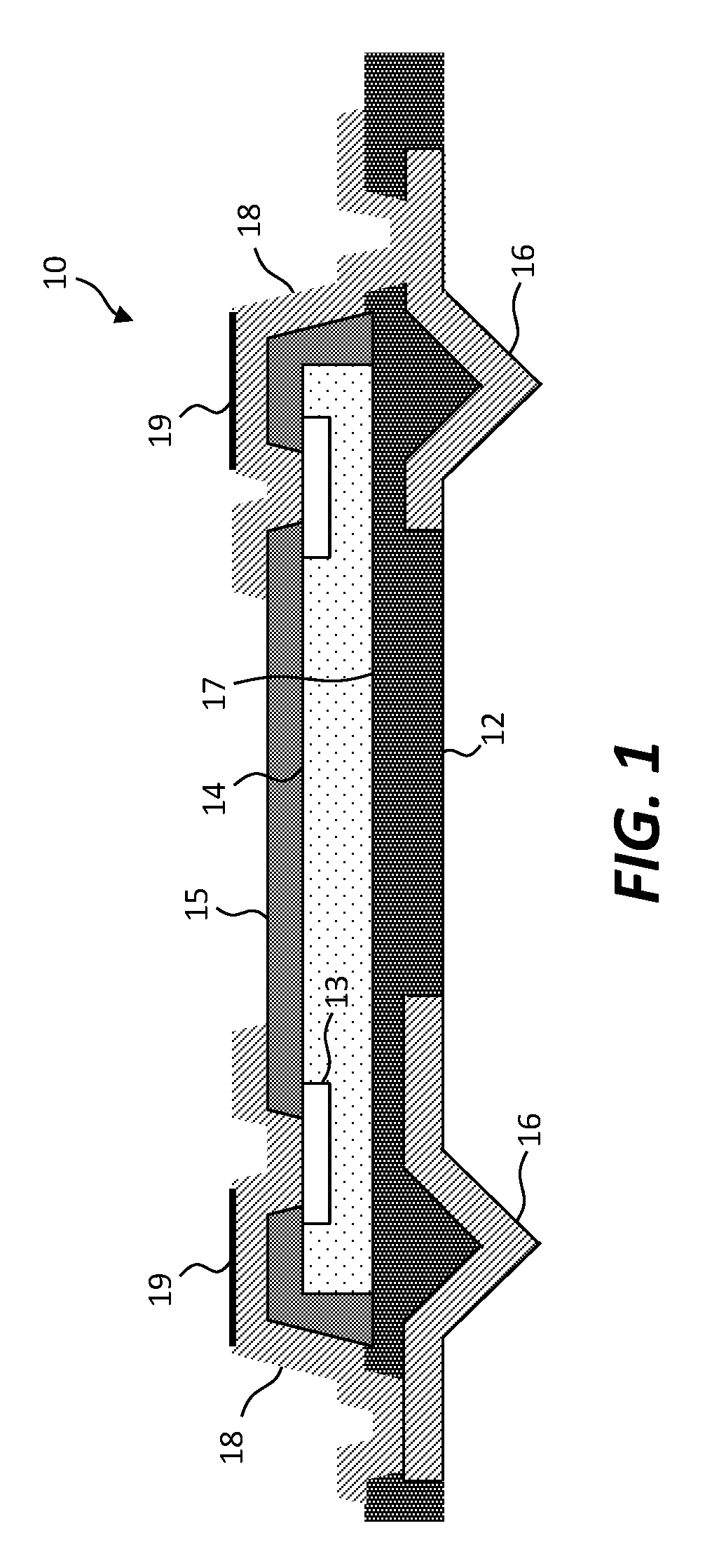
[0050]Referring to the cross section of FIG. 1, in some embodiments of the present invention, a printable (e.g., micro-transfer printable) electronic component 10 or printed electronic component 10 (hereinafter component 10) includes a component substrate 12 and a circuit 14 disposed in or on the component substrate 12, for example disposed on a component surface 17 of the component substrate 12. The circuit 14 can include or be electricall...


PUM


Abstract

A printable electronic component includes a component substrate and a circuit disposed in or on the component substrate. One or more electrically conductive connection posts protrude from the component substrate. One or more electrically conductive component contact pads are exposed on or over the component substrate on a side of the component substrate opposite the one or more connection posts. The one or more component contact pads and the one or more electrically conductive connection posts are both electrically connected to the circuit. The components can be printed onto a destination substrate and electrically connected to contact pads on the destination substrate through the connection posts. The components can also be printed onto other components and electrically connected through the connection posts and component contact pads to form a three-dimensional electronic structure.

Description

PRIORITY APPLICATION[0001]This application claims priority to and benefit of U.S. Provisional Patent Application No. 62 / 371,008, filed Aug. 4, 2016, entitled Printable 3D Electronic Structure, the disclosure of which is hereby incorporated by reference in its entirety.CROSS REFERENCE TO RELATED APPLICATIONS[0002]Reference is made to U.S. Pat. No. 8,889,485, entitled Methods for Surface Attachment of Flipped Active Components by Christopher Bower, U.S. patent application Ser. No. 14 / 743,788, entitled Micro Assembled LED Displays and Lighting Elements by Christopher Bower et al., and U.S. patent application Ser. No. 14 / 822,864, entitled Chiplets with Connection Posts by Prevatte et al., the disclosures of which are incorporated herein by reference in its entirety.FIELD OF THE INVENTION[0003]The present invention relates generally to structures and methods for electrically interconnecting chiplets using micro-transfer printing.BACKGROUND OF THE INVENTION[0004]Substrates with electronic...

Claims


Application Information

Patent Timeline
IPC IPC(8): H05K1/18H01L23/00H01G4/38H01L23/498H01L23/31H01L25/16H01L21/683H01L21/48
CPCH05K1/18H01L21/6835H01L24/02H01L21/4853H01L21/481H01L23/49833H01L23/49811H01L23/3114H01L25/16H01G4/38H01L2221/68318H01L2221/68345H01L2221/68359H01L2224/02311H01L2224/02371H01L2224/02381H05K2201/10166H01L25/105H05K1/141H05K1/144H05K1/162H05K3/4007H05K3/4682H01L2225/1035H01L2225/1076H05K2201/0367H05K2201/045H05K2201/09672H05K2201/10515H05K2201/10522H05K2201/1053H05K2201/2072H05K2203/0165H05K2203/0278H05K2203/302H05K2203/308H01G4/33H01L23/13H01L21/4867H01L24/19H01L24/20H01L2224/18H01L2224/2101H01L2224/2105H01L2224/211H01L2221/6835H01L2221/68368H01L2221/68381H01L2924/0001
Inventor COK, RONALD S.
Owner X DISPLAY CO TECH LTD
Why Eureka
Try Eureka