Polycrystalline ceramic substrate and method of manufacture

a technology of polycrystalline ceramics and substrates, applied in the direction of polycrystalline material growth, crystal growth process, coatings, etc., can solve the problems of substrate cracking, material creep, and inability to perform additional lithographic steps necessary for device fabrication, so as to reduce stress, increase dislocation density, and improve the effect of electrical and optical properties of the epitaxial layer

Active Publication Date: 2018-02-15
QROMIS INC
View PDF4 Cites 23 Cited by
  • Summary
  • Abstract
  • Description
  • Claims
  • Application Information

AI Technical Summary

Benefits of technology

[0007]Numerous benefits are achieved by way of the present invention over conventional techniques. For example, embodiments of the present invention provide substrate structure suitable for epitaxial growth that is characterized by a coefficient of thermal expansion (CTE) that is substantially matched to epitaxial layers grown thereon. Matching the thermal expansion properties of the growth substrate to the epitaxial layer reduces the stress in the epitaxial layers and / or the engineered substrate. Stress is responsible for several types of defects. For example, stress may increase dislocation density in the epitaxial layer, which impairs electrical and optical properties of the epitaxial layer. Stress may also lead to residual strain in the epitaxial layer or the substrate, which may lead to additional processing concern in later steps, such as stress cracking, dislocation glide, slip, bow and warp. Thermal expansion induced bow and warp of the substrate may make handling of the material problematic in automated equipment, and limit the ability to perform additional lithographic steps necessary for device fabrication, substrate cracking, and materials creep. In addition, the device performance lifetime is reduced in stressed materials. Stress relaxation and stress-induced crack propagation, dislocation glide, and other lattice movement resulting from thermal mismatch may lead to early failures in a range of modes, from reduced device performance to fracture or peeling of devices and device layers. The devices are manufactured in the epitaxial layers.

Problems solved by technology

For example, stress may increase dislocation density in the epitaxial layer, which impairs electrical and optical properties of the epitaxial layer.
Stress may also lead to residual strain in the epitaxial layer or the substrate, which may lead to additional processing concern in later steps, such as stress cracking, dislocation glide, slip, bow and warp.
Thermal expansion induced bow and warp of the substrate may make handling of the material problematic in automated equipment, and limit the ability to perform additional lithographic steps necessary for device fabrication, substrate cracking, and materials creep.
In addition, the device performance lifetime is reduced in stressed materials.
Stress relaxation and stress-induced crack propagation, dislocation glide, and other lattice movement resulting from thermal mismatch may lead to early failures in a range of modes, from reduced device performance to fracture or peeling of devices and device layers.

Method used


Image

  • Polycrystalline ceramic substrate and method of manufacture
  • Polycrystalline ceramic substrate and method of manufacture
  • Polycrystalline ceramic substrate and method of manufacture

Examples


Embodiment Construction

[0027]Embodiments of the present invention relate to engineered substrate structures. More specifically, the present invention relates to methods and systems suitable for use in epitaxial growth processes. Merely by way of example, the invention has been applied to a method and system for providing a substrate structure suitable for epitaxial growth that is characterized by a coefficient of thermal expansion (CTE) that is substantially matched to epitaxial layers grown thereon. The methods and techniques can be applied to a variety of semiconductor processing operations.

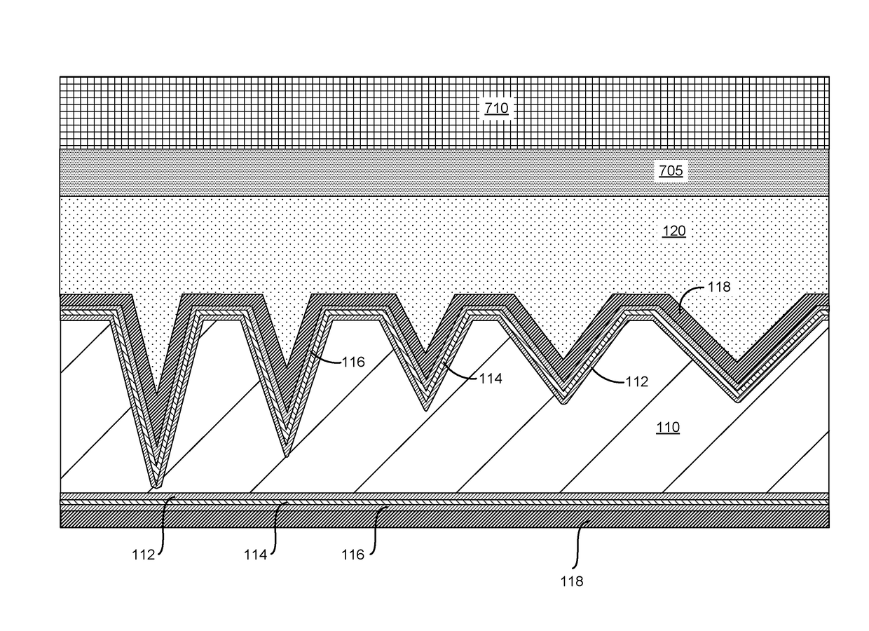
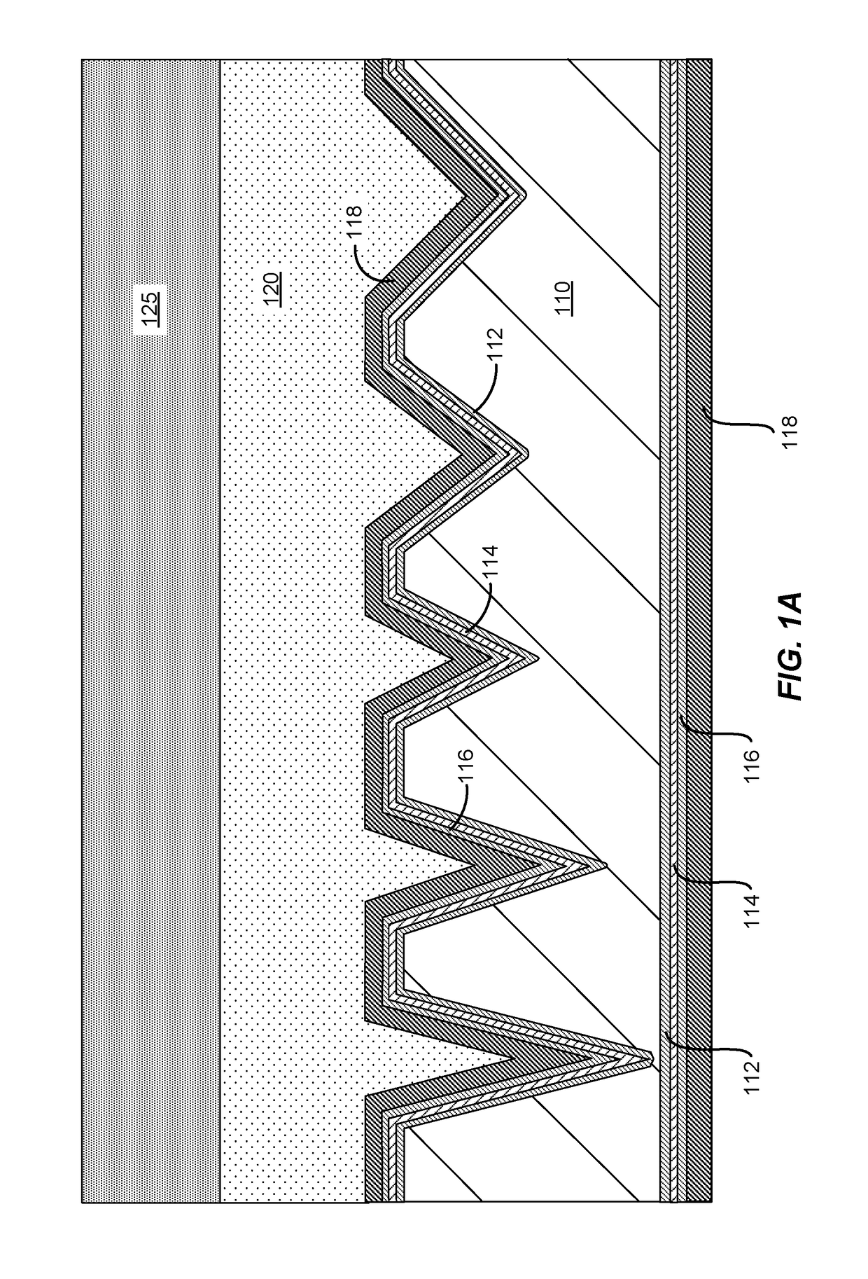
[0028]FIG. 1A is a simplified schematic diagram illustrating an engineered substrate structure according to an embodiment of the present invention. As illustrated in FIG. 1A, the engineered substrate structure illustrated in FIG. 1A is suitable for a variety of electronic and optical applications. The engineered substrate structure includes a core 110 (e.g., AlN Substrate) that can have a coefficient of thermal expan...


PUM

PropertyMeasurementUnit
RMS roughnessaaaaaaaaaa
thicknessaaaaaaaaaa

Abstract

A method of fabricating a ceramic substrate structure includes providing a ceramic substrate, encapsulating the ceramic substrate in a barrier layer, and forming a bonding layer coupled to the barrier layer. The method further includes removing a portion of the bonding layer to expose at least a portion of the barrier layer and define fill regions, and depositing a second bonding layer on the at least a portion of the exposed barrier layer and the fill regions.

Description

CROSS-REFERENCES TO RELATED APPLICATIONS[0001]This application claims priority to U.S. Provisional Patent Application No. 62 / 354,623, filed on Jun. 24, 2016, entitled “POLYCRYSTALLINE CERAMIC SUBSTRATE AND METHOD OF MANUFACTURE,” the disclosure of which is hereby incorporated by reference in its entirety for all purposes.BACKGROUND OF THE INVENTION[0002]Light-emitting diode (LED) structures are typically epitaxially grown on sapphire substrates. Many products currently use LED devices, including lighting, computer monitors, and other display devices.[0003]The growth of gallium nitride based LED structures on a sapphire substrate is a heteroepitaxial growth process since the substrate and the epitaxial layers are composed of different materials. Due to the heteroepitaxial growth process, the epitaxially grown material can exhibit a variety of adverse effects, including reduced uniformity and reductions in metrics associated with the electronic / optical properties of the epitaxial laye...

Claims


Application Information

Patent Timeline
Patent Type & Authority Applications(United States)
IPC IPC(8): H01L21/02C23C16/56C23C16/40C23C16/50C30B29/06C30B29/40
CPCH01L21/0242H01L21/0243H01L21/0245H01L21/02516H01L21/02532H01L21/0254C30B29/06C30B29/406C23C16/401C23C16/50C23C16/56H01L33/0075H01L33/20H01L33/12H01L33/0093H01L21/02002H01L21/2007H01L21/84H01L27/12H01L33/02C30B29/403
Inventor ODNOBLYUDOV, VLADIMIRBASCERI, CEMFARRENS, SHARI
Owner QROMIS INC
Why Eureka
Try Eureka