Display device and electronic device

Active Publication Date: 2018-03-01
SEMICON ENERGY LAB CO LTD
View PDF14 Cites 27 Cited by
  • Summary
  • Abstract
  • Description
  • Claims
  • Application Information

AI Technical Summary

Benefits of technology

[0011]In a display device including one type of a display element, using a transistor including a metal oxide or an oxide semiconductor in a channel formation region (hereinafter, the transistor is referred to as “OS transistor”) for a pixel circuit including a display element, a driver circuit, or the like has been proposed. The OS transistor has a characteristic of extremely low off-state current. Thus, when the OS transistor is used for a pixel circuit, for exampl

Problems solved by technology

However, the conditions of heat treatment, such as a temperature, a time, and an atmosphere, are different between a process for forming the OS transistor and a process for forming the Si transi

Method used


Image

  • Display device and electronic device
  • Display device and electronic device
  • Display device and electronic device

Examples


Example

Embodiment 1

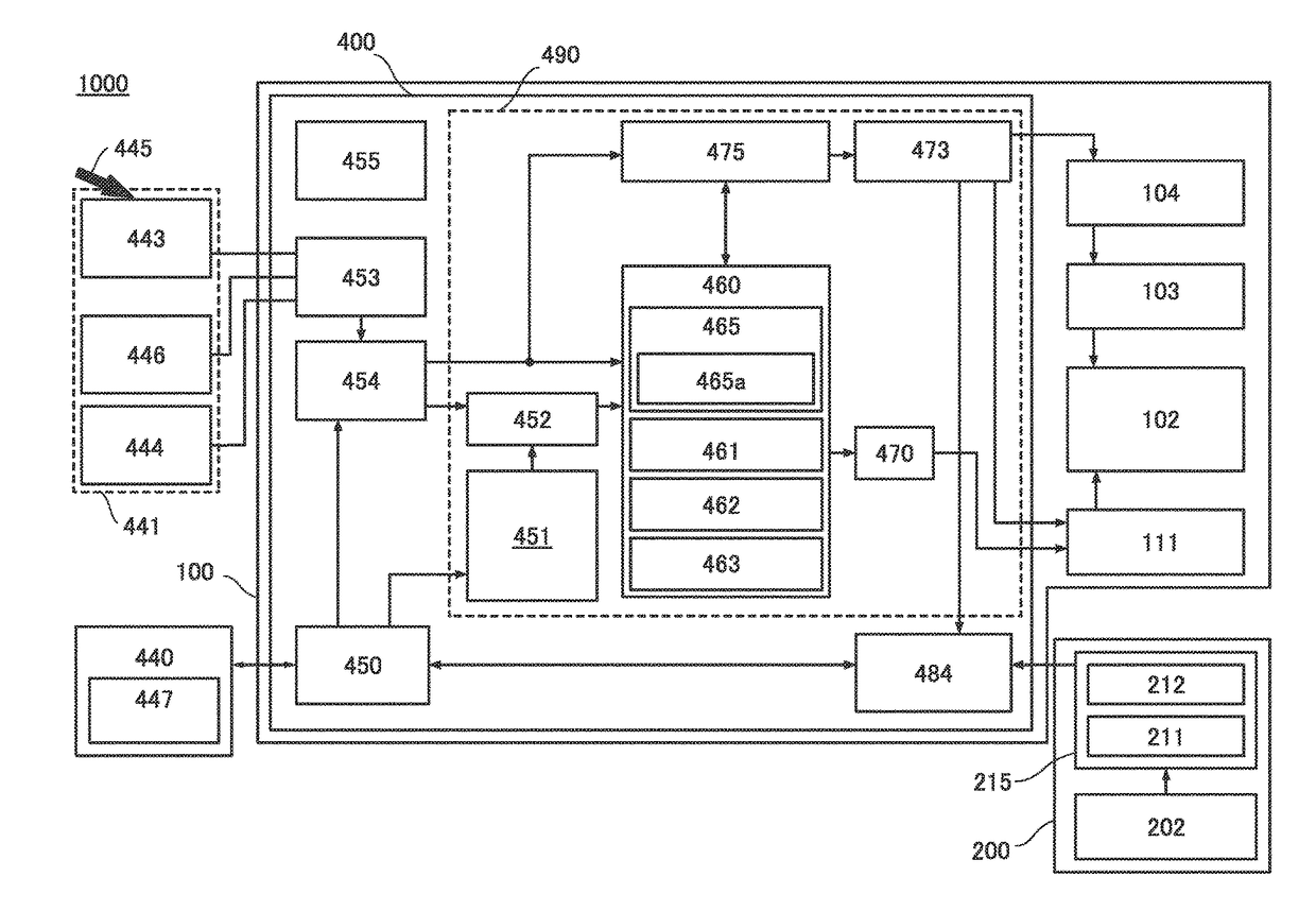
[0092]In this embodiment, a structure of a display device of one embodiment of the present invention will be described.

[0093]FIG. 1 is a block diagram showing a configuration example of a display device 1000. The display device 1000 includes a display unit 100, a touch sensor unit 200, a sensor 441, and a host device 440. In particular, the details of a controller IC (integrated circuit) 400 included in the display unit 100 are shown. The display unit 100 is a display unit including one of a liquid crystal element, a light-emitting element, and the like as a display element.

[0094]The display unit 100 includes a display portion 102, a gate driver 103, a level shifter 104, and a source driver IC 111 in addition to the controller IC 400. Note that the display element is included in the display portion 102.

[0095]The controller IC 400 includes an interface 450, a frame memory 451, a decoder 452, a sensor controller 453, a controller 454, a clock generation circuit 455, an ima...

Example

Embodiment 2

[0186]In this embodiment, a method for correcting an image using the host device 440, the sensor 441, and the image processing portion 460 in the controller IC 400 or 400A described in Embodiment 1 will be described. Note that for the method for correcting an image, a neural network is used.

[0187]A neural network is an information processing system modeled on a biological neural network. A computer having a higher performance than a conventional Neumann computer is expected to be provided by utilizing the neural network, and in these years, a variety of researches on a neural network formed over an electronic circuit have been carried out.

[0188]In the neural network, units which resemble neurons are connected to each other through units which resemble synapses. By changing the connection strength, a variety of input patterns are learned, and pattern recognition, associative storage, or the like can be performed at high speed.

[0189]For example, a product-sum operation cir...

Example

Example 1 of Circuit for Constructing Hierarchical Neural Network

[0211]Next, a configuration example of a product-sum operation circuit for constructing the above-described hierarchical neural network will be described.

[0212]FIG. 11 is a block diagram of the semiconductor device 700 that serves as a product-sum operation circuit. The semiconductor device 700 includes an offset circuit 710 and a memory cell array 720.

[0213]The offset circuit 710 includes column output circuits OUT[1] to OUT[n] (here, n is an integer greater than or equal to 1) and a reference column output circuit Cref.

[0214]In the memory cell array 720, m (here, m is an integer greater than or equal to 1) memory cells AM are arranged in the column direction and n memory cells AM are arranged in the row direction; that is, m×n memory cells AM are provided. The total number of the memory cells AM and the memory cells AMref arranged in a matrix in the memory cell array 720 is m×(n+1). In particular, in the memory cell ...


PUM


Abstract

A display device that performs image correction in accordance with external light environment is provided. The display device includes a host device and an optical sensor. In addition, the display device includes a processing circuit. The host device has a function of performing arithmetic processing using a neural network on software and a function of performing supervised learning with the neural network. The processing circuit has a function of performing arithmetic processing using a neural network on hardware. The optical sensor has a function of obtaining illuminance of external light. The obtained illuminance of external light is inputted to the host device, and a luminance and color tone preferred by users are regarded as teacher data, whereby learning is performed on the neural network of the host device. A weight coefficient obtained through the learning is used as a weight coefficient of the neural network of the processing circuit. By inputting illuminance of external light to the processing circuit, set values of luminance and color tone selected by the users are calculated in the neural network of the processing circuit.

Description

TECHNICAL FIELD[0001]One embodiment of the present invention relates to a display device and an electronic device.[0002]Note that one embodiment of the present invention is not limited to the above technical field. The technical field of the invention disclosed in this specification and the like relates to an object, a method, or a manufacturing method. In addition, one embodiment of the present invention relates to a process, a machine, manufacture, or a composition of matter. Specifically, examples of the technical field of one embodiment of the present invention disclosed in this specification include a semiconductor device, a display device, a liquid crystal display device, a light-emitting device, a power storage device, an imaging device, a memory device, a processor, an electronic device, a method for driving any of them, a method for manufacturing any of them, a method for testing any of them, and a system including any of them.BACKGROUND ART[0003]Display devices included in...

Claims


Application Information

Patent Timeline
IPC IPC(8): G09G3/36G09G3/3233
CPCG09G3/3648G09G3/3233G09G2360/144G09G3/367G09G2300/0465G09G3/3629
Inventor KUROKAWA, YOSHIYUKI
Owner SEMICON ENERGY LAB CO LTD
Why Eureka
Try Eureka