Defect Marking For Semiconductor Wafer Inspection

a technology of defect marking and semiconductor wafer, which is applied in the direction of semiconductor/solid-state device testing/measurement, instruments, material analysis, etc., can solve the problem that the electron beam based measurement system cannot directly detect or verify defects buried in relatively thick semiconductor structures, and achieve accurate measurement of distance and accurate location of buried defects

Inactive Publication Date: 2018-03-29
KLA TENCOR TECH CORP
View PDF0 Cites 9 Cited by
  • Summary
  • Abstract
  • Description
  • Claims
  • Application Information

AI Technical Summary

Benefits of technology

[0015]Methods and systems for accurately locating buried defects previously detected by an optical or x-ray inspection system are described herein. In one aspect, a physical mark is made on the surface of a...

Problems solved by technology

The electron-beam based measurement system cannot directly detect...

Method used


Image

  • Defect Marking For Semiconductor Wafer Inspection
  • Defect Marking For Semiconductor Wafer Inspection
  • Defect Marking For Semiconductor Wafer Inspection

Examples


Embodiment Construction

[0034]Reference will now be made in detail to background examples and some embodiments of the invention, examples of which are illustrated in the accompanying drawings.

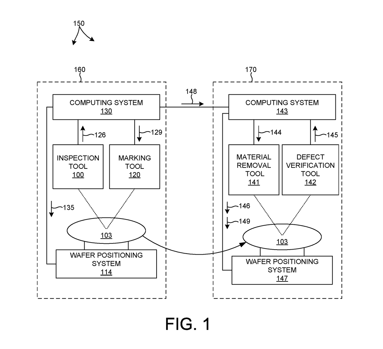
[0035]Methods and systems for accurately locating buried defects previously detected by an optical or x-ray inspection system are described herein.

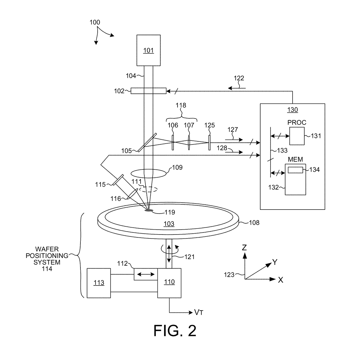
[0036]In one aspect, a physical mark is made on the surface of a wafer near a buried defect detected by an inspection system. In addition, the inspection system is employed to accurately measure the distance between the detected defect and the physical mark in at least two dimensions. The wafer, an indication of the nominal location of the mark, and an indication of the distance between the detected defect and the mark are transferred to a defect verification tool. In some embodiments, the defect verification tool is an x-ray based measurement system. In some embodiments, the defect verification tool is an electron beam based measurement system. In some of these embodiments...


PUM


Abstract

Methods and systems for accurately locating buried defects previously detected by an inspection system are described herein. A physical mark is made on the surface of a wafer near a buried defect detected by an inspection system. In addition, the inspection system accurately measures the distance between the detected defect and the physical mark in at least two dimensions. The wafer, an indication of the nominal location of the mark, and an indication of the distance between the detected defect and the mark are transferred to a material removal tool. The material removal tool (e.g., a focused ion beam (FIB) machining tool) removes material from the surface of the wafer above the buried defect until the buried defect is made visible to an electron-beam based measurement system. The electron-beam based measurement system is subsequently employed to further analyze the defect.

Description

CROSS REFERENCE TO RELATED APPLICATION[0001]The present application for patent claims priority under 35 U.S.C. § 119 from U.S. provisional patent application Ser. No. 62 / 400,182, filed Sep. 27, 2016, entitled “Defect Marking for Semiconductor Wafer Inspection,” the subject matter of which is incorporated herein by reference in its entirety.TECHNICAL FIELD[0002]The described embodiments relate to systems for surface inspection, and more particularly to semiconductor wafer inspection modalities.BACKGROUND INFORMATION[0003]Semiconductor devices such as logic and memory devices are typically fabricated by a sequence of processing steps applied to a substrate or wafer. The various features and multiple structural levels of the semiconductor devices are formed by these processing steps. For example, lithography among others is one semiconductor fabrication process that involves generating a pattern on a semiconductor wafer. Additional examples of semiconductor fabrication processes includ...

Claims


Application Information

Patent Timeline
IPC IPC(8): G01N21/88G01N1/28G01N1/44G01N21/95
CPCG01N21/8851G01N1/286G01N21/9501G01N21/8806G01N1/44G01N21/9506G01N21/956G01N2021/888H01L21/67259H01L21/67282H01L22/12H01L22/30
Inventor SHORTT, DAVIDLANGE, STEVENWEI, JUNWEIKAPP, DANIELAMSDEN, CHARLES
Owner KLA TENCOR TECH CORP
Why Eureka
Try Eureka