High-frequency module

a high-frequency module and shield layer technology, applied in the field of modules, can solve the problems of difficult depositing metal onto the bottom portion of the slit and reduce the resistance of the shield layer, so as to improve the shield layer characteristics, improve the performance of the high-frequency module, and improve the effect of shield layer characteristics

Active Publication Date: 2018-03-29
MURATA MFG CO LTD
View PDF10 Cites 32 Cited by
  • Summary
  • Abstract
  • Description
  • Claims
  • Application Information

AI Technical Summary

Benefits of technology

[0008]In recent years, there has been a demand to further improve the characteristics of the shield layer as performance of the high-frequency module increases. To improve the shield characteristics, it is necessary to lower the resistance of the shield layer and to reduce the coupling resistance between the shield layer and the ground electrode. However, since the conductive resin that forms the above-described shield layer 104 is obtained, for example, by adding a metal filler to an epoxy resin, the specific resistance thereof is higher than that of the metal filler alone. Accordingly, for example, it is conceivable to fill the slit S with metal by a film deposition technology such as sputtering. However, if the slit S is deep, it is difficult to deposit a metal onto a bottom portion of the slit S and to lower the resistance of the shield layer.

Problems solved by technology

However, if the slit S is deep, it is difficult to deposit a metal onto a bottom portion of the slit S and to lower the resistance of the shield layer.

Method used


Image

  • High-frequency module
  • High-frequency module
  • High-frequency module

Examples


first embodiment

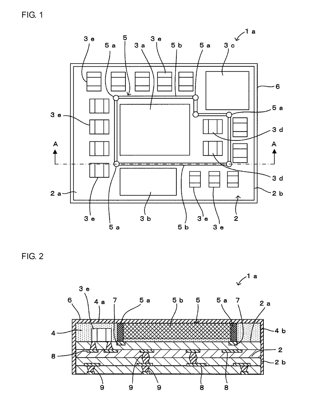
[0057]A high-frequency module 1a according to the present disclosure will be described with reference to FIGS. 1 and 2. FIG. 1 is a plan view of the high-frequency module, and FIG. 2 is a cross-sectional view on arrow A-A in FIG. 1. In FIG. 1, a top surface portion of a shield film 6 and a sealing resin layer 4 are not illustrated.

[0058]As illustrated in FIGS. 1 and 2, the high-frequency module la according to this embodiment includes a wiring board 2, a plurality of components 3a and 3b mounted on an upper surface 2a of the wiring board 2, a sealing resin layer 4 stacked on the upper surface 2a of the wiring board 2, a shield film 6 that covers a surface of the sealing resin layer 4, and a shield wall 5 provided inside the sealing resin layer 4, and is mounted on, for example, a motherboard of an electronic device in which a high-frequency signal is used.

[0059]The wiring board 2 is made of, for example, a low-temperature co-fired ceramic material or glass epoxy resin. The upper sur...

second embodiment

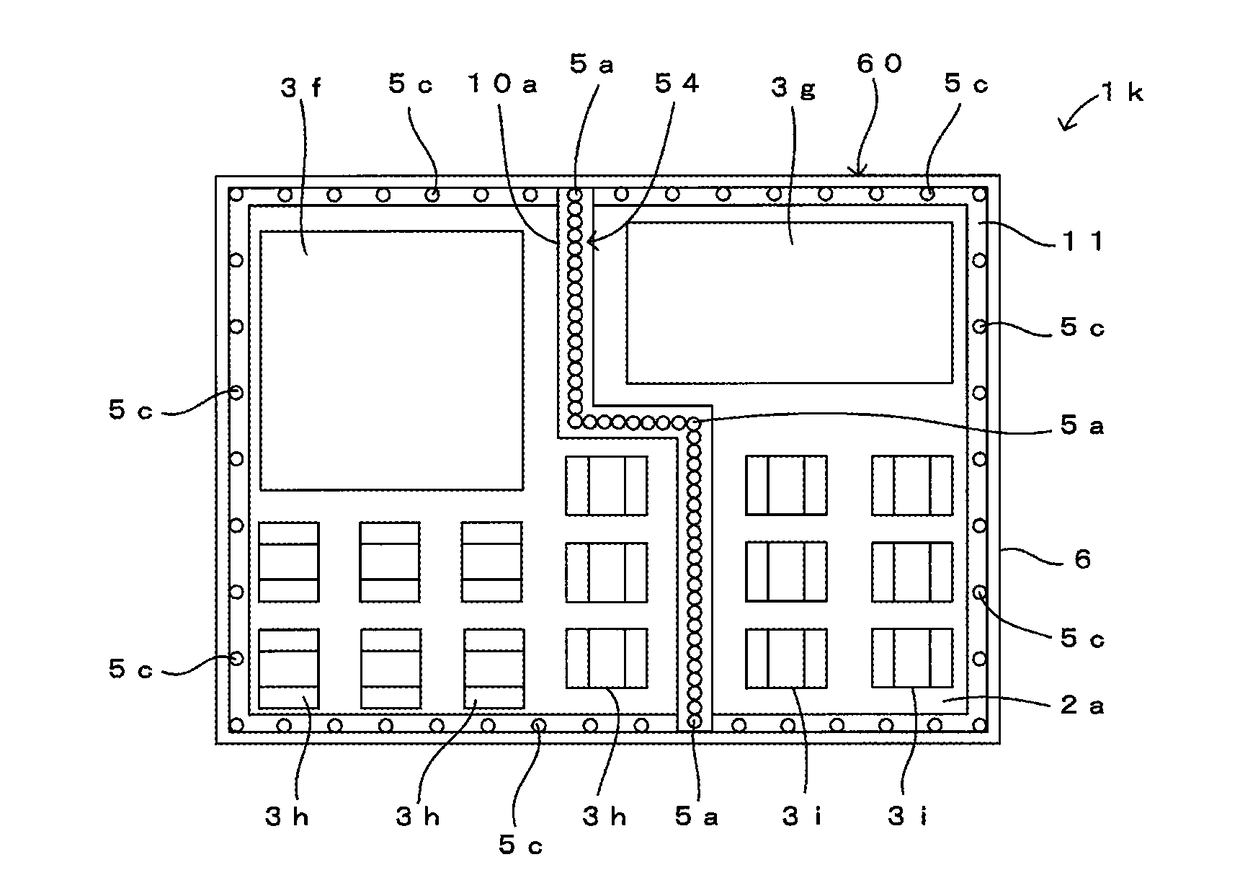
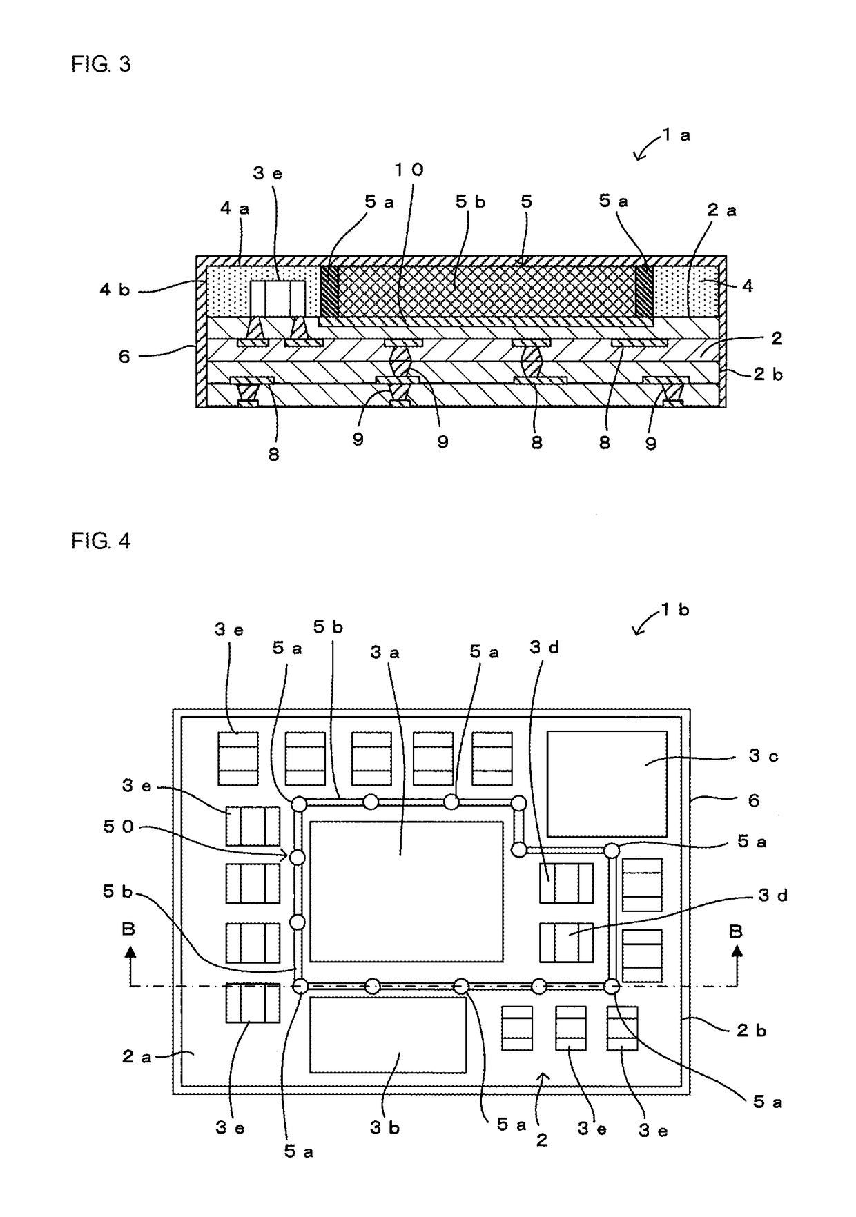
[0082]A high-frequency module 1b according to the present disclosure will be described with reference to FIGS. 4 and 5. FIG. 4 is a plan view of the high-frequency module 1b, and FIG. 5 is a cross-sectional view on arrow B-B in FIG. 4. In FIG. 4, a top surface portion of a shield film 6 and a sealing resin layer 4 are not illustrated.

[0083]The high-frequency module 1b of this embodiment is different from the high-frequency module 1a of the first embodiment described with reference to FIGS. 1 and 2 in the structure of a shield wall 50, as illustrated in FIGS. 4 and 5. Since other structures are the same as those of the high-frequency module 1a of the first embodiment, they are denoted by the same reference numerals, and descriptions thereof are thereby skipped.

[0084]In this case, in a plan view, a plurality of metal pins 5a are also disposed in portions other than bent portions of the shield wall 50. Further, land electrodes 7 are provided at respective mount portions of the metal pi...

third embodiment

[0089]A high-frequency mode 1c according to the present disclosure will be described with reference to FIG. 7. FIG. 7 is a plan view of the high-frequency module 1c, and corresponds to FIG. 1.

[0090]The high-frequency module 1c of this embodiment is different from the high-frequency module 1a of the first embodiment described with reference to FIGS. 1 and 2 in the structure of a shield wall 51, as illustrated in FIG. 7. Since other structures are the same as those of the high-frequency module 1a of the first embodiment, they are denoted by the same signs and descriptions thereof are thereby skipped.

[0091]While the above-described shield wall 5 of the first embodiment is disposed to surround the components 3a and 3d located in the center portion of the upper surface 2a of the wiring board 2, the shield wall 51 of this embodiment is disposed to divide the upper surface 2a of the wiring board 2 into two regions. In this way, the arrangement of the shield wall 51 may be appropriately cha...


PUM


Abstract

The characteristics of a shield wall that prevents the mutual interference of the noise between components are improved by lowering the resistance of the shield wall. A high-frequency module 1a includes a wiring board 2, a plurality of components 3a to 3e mounted on an upper surface 2a of the wiring board 2, a sealing resin layer 4 stacked on the upper surface 2a of the wiring board 2 to seal the components 3a to 3e, and a shield wall 5 disposed between the adjacent components in the sealing resin layer 4. A part of the shield wall 5 is constituted of metal pins 5a standing on the upper surface 2a of the wiring board 2.

Description

[0001]This is a continuation of International Application No. PCT / JP2016 / 063830 filed on May 10, 2016 which claims priority from Japanese Patent Application No. 2015-243853 filed on Dec. 15, 2015 and Japanese Patent Application No. 2015-096508 filed on May 11, 2015. The contents of these applications are incorporated herein by reference in their entireties.FIELD OF THE DISCLOSURE[0002]The present disclosure relates to a module including a sealing resin layer that covers a component mounted on a wiring board and a shield layer stacked on the sealing resin layer.DESCRIPTION OF THE RELATED ART[0003]High-frequency modules mounted in, for example, mobile terminal devices sometimes include a shield layer for blocking electromagnetic waves. In some modules of this type, a component mounted on a wiring board is covered with a molding resin and a shield layer is provided to cover a surface of the molding resin.[0004]A shield layer is provided to block external noise. When a plurality of comp...

Claims


Application Information

Patent Timeline
Patent Type & Authority Applications(United States)
IPC IPC(8): H05K9/00H05K1/18H05K5/06H01L23/552
CPCH05K9/0024H05K1/181H05K5/065H01L23/552H05K2201/10522H05K2201/10318H01L25/0655H01L24/16H01L2224/16227H01L23/5383H01L23/3121H01L2924/19105H01L2924/181H01L2224/16225H05K1/0218H05K3/284H01L23/66H01L24/13H01L24/81H01L2224/13101H01L2224/81801H01L23/5384H01L2924/3025H01L23/18H01L23/3135Y02P70/50H01L2924/00012H01L2924/014H01L2924/00014H01L23/28
Inventor OTSUBO, YOSHIHITOYAMAMOTO, ISSEI
Owner MURATA MFG CO LTD
Why Eureka
Try Eureka