Power transmission device and wireless power transfer system

a wireless power transfer and transmission device technology, applied in the direction of electrical equipment, semiconductor devices, circuit arrangements, etc., can solve the problems of increasing the design is complicated, and the difficulty in reducing the size of the power transmission device, so as to achieve simple wireless power transfer, small size, and low cost.

Active Publication Date: 2018-05-10
MURATA MFG CO LTD
View PDF3 Cites 0 Cited by
  • Summary
  • Abstract
  • Description
  • Claims
  • Application Information

AI Technical Summary

Benefits of technology

[0020]The above-described advantageous effects can thus be obtained.
[0021](2) In the above configuration (1), it is preferable that at least a portion of the control circuit section and at least a portion of the power circuit section be formed of a complementary metal oxide semiconductor (CMOS) standard logic integrated circuit (IC) or a transistor-transistor logic (TTL) standard logic IC that includes a plurality of logic gate circuits and that is sealed in a single small-sized package with a plurality of terminals. As a result, an overwhelmingly inexpensive power transmission device can be fabricated by forming the power transmission device by using a standard logic IC, which is widely distributed in the market. In addition, unprecedentedly and overwhelmingly small-sized, simple wireless power transfer can be realized.
[0022](3) In the above configuration (2), it is preferable that the CMOS standard logic IC or the TTL standard logic IC include four two-input NAND gates. As a result, the power transmission device can be formed by using a single standard logic IC. In addition, an overwhelmingly inexpensive and simple power transmission device can be formed.
[0023](4) In the above configuration (3), it is preferable that the control circuit section include an oscillation circuit that includes one of the four NAND gates and an oscillator and that the power circuit section include the remaining NAND gates among the four NAND gates. As a result, both the control circuit section and the power circuit section can be formed by using a standard logic IC, and a circuit within the standard logic IC can be effectively used.
[0024](5) In the above configuration (4), it is preferable that, in the control circuit section, one of the remaining NAND gates (that is not connected in parallel) be connected to an output unit of the oscillation circuit. As a result, a waveform is shaped by the one NAND gate (driving circuit unit), and a switching operation is performed by the power circuit section at an appropriate timing, so that larger electric power can be handled. In addition, concentration of power loss that is generated as a result of the switching operation being performed by the power circuit section at an inappropriate timing can be suppressed.
[0025](6) In the above configurations (4) or (5), it is preferable that some of the remaining NAND gates be connected in parallel. As a result, the current-carrying capacity of the power circuit section is increased, and larger electric power can be handled.

Problems solved by technology

(1) The power transmission circuit 11 has a large-scale circuit configuration, and it is difficult to reduce the size of the power transmission device.
Consequently, the size of the power transmission device increases.
Thus, it is necessary to take measures against the electromagnetic noise for each design of the power transmission circuit 11, and the design is complicated.
Thus, the footprints of the power semiconductor devices Q1 and Q2 are large, and it is difficult to reduce the size of the power transmission circuit 11.
Thus, in the case of trying to level out and dissipate the heat generated by the power semiconductor devices Q1 and Q2, the structure for levelling out and dissipating the heat becomes complex, and this makes it difficult to reduce the size of the power transmission circuit 11.

Method used


Image

  • Power transmission device and wireless power transfer system
  • Power transmission device and wireless power transfer system
  • Power transmission device and wireless power transfer system

Examples


first embodiment

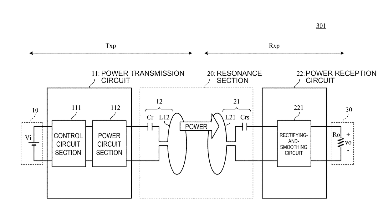
[0077]FIG. 1 is a block diagram of a wireless power transfer system 301 according to a first embodiment. The wireless power transfer system includes a power transmission device Txp and a power reception device Rxp. The power transmission device Txp includes a power transmission coil L12, a power-transmission resonance capacitor Cr that forms, together with the power transmission coil L12, a power-transmission resonance mechanism 12, and a power transmission circuit 11 that is electrically connected to the power-transmission resonance mechanism 12 and that intermittently applies a DC input voltage to the power-transmission resonance mechanism 12 and causes the power transmission coil L12 to generate an AC voltage. The power reception device Rxp includes a power reception coil L21, a power-reception resonance capacitor Crs that forms a power-reception resonance mechanism 21 with the power reception coil L21, and a power reception circuit 22 that is electrically connected to the power-...

second embodiment

[0108]In a second embodiment, a power transmission circuit formed on a very small single circuit board will be described.

[0109]FIG. 6A is a circuit diagram of a power transmission device according to the second embodiment, and FIG. 6B is a diagram illustrating the connection relationship between components including an IC in the circuit illustrated in FIG. 6A. FIG. 7 is a plan view of a circuit board on which the power transmission circuit has been formed. An input power supply of, for example, 5 V is connected to a connector CN1. The power transmission coil L12 is connected to a connector CN2. A circuit that includes a light emitting diode (LED) and a resistor R1, the LED indicating application of a voltage by the input power supply, is connected between a power line and a ground. A smoothing capacitor C11 and a high-frequency filter capacitor C12 are also connected between the power line and the ground. In addition, a standard logic IC (IC4) is connected between the power line and...

third embodiment

[0111]In a third embodiment, a case will be described in which a power circuit section has a configuration different from that according to the second embodiment.

[0112]FIG. 8A is a circuit diagram of a power transmission device according to the third embodiment, and FIG. 8B is a diagram illustrating the connection relationship between components including an IC in the circuit illustrated in FIG. 8A. FIG. 9 is a plan view of a circuit board on which a power transmission circuit according to the third embodiment has been formed. An input power supply of, for example, 5 V is connected to the connector CN1. The power transmission coil L12 is connected to the connector CN2.

[0113]An oscillation circuit OSC is a single component that includes the oscillator XO and a buffer amplifier AMP. A circuit that includes an LED and the resistor R1 is connected between a power line and a power supply terminal of the oscillation circuit OSC. A smoothing capacitor C2 is connected between the power supp...


PUM


Abstract

A power transmission device includes a power transmission coil, a power-transmission resonance capacitor that forms, together with the power transmission coil, a power-transmission resonance mechanism, and a power transmission circuit electrically connected to the power-transmission resonance mechanism that intermittently applies a direct-current input voltage to the power-transmission resonance mechanism and causes the power transmission coil to generate an alternating-current voltage. The power transmission circuit includes a control circuit section including an oscillator, and a power circuit section formed of an integrated circuit sealed in a small-sized package with a plurality of terminals. The integrated circuit is electrically and directly connected to the power-transmission resonance mechanism. The control circuit section oscillates at a predetermined frequency and outputs a driving signal which is input to the power circuit section. The power circuit section intermittently applies a direct-current voltage to the power-transmission resonance mechanism using a transistor in the integrated circuit.

Description

CROSS-REFERENCE TO RELATED APPLICATION[0001]This application claims benefit of priority to International Patent Application No. PCT / JP2016 / 069218, filed Jun. 29, 2016, and to Japanese Patent Application No. 2015-138925, filed Jul. 10, 2015, the entire contents of each are incorporated herein by reference.BACKGROUNDTechnical Field[0002]The present disclosure relates to a wireless power transfer apparatus that includes a power transmission device, which includes a power transmission coil, and a power reception device, which includes a power reception coil, and in which power is wirelessly transferred from the power transmission device to the power reception device.Background Art[0003]In recent years, research and development for reducing power loss in the entire system has been actively conducted with the aim of putting wireless power transfer into practical use. In particular, in a system in which an electromagnetic resonance field is formed and in which wireless power transfer is pe...

Claims


Application Information

Patent Timeline
Patent Type & Authority Applications(United States)
IPC IPC(8): H02J50/12H02J5/00H01L29/74
CPCH02J50/12H02J5/005H01L29/742
Inventor HOSOTANI, TATSUYA
Owner MURATA MFG CO LTD
Why Eureka
Try Eureka