Wafer noise reduction by image subtraction across layers

a layer and image technology, applied in image enhancement, semiconductor/solid-state device testing/measurement, instruments, etc., can solve the problems of reducing the size of defects, the operation of semiconductor manufacturing processes closer to the limitation of process performance capability, and the impact of smaller defects on the electrical parameters of the device, so as to achieve noise reduction and image noise reduction

Active Publication Date: 2018-05-24
KLA TENCOR TECH CORP
View PDF0 Cites 10 Cited by
  • Summary
  • Abstract
  • Description
  • Claims
  • Application Information

AI Technical Summary

Benefits of technology

[0008]In a first embodiment, a method for noise reduction during defect identification in a multi-layered wafer is provided. The method comprises a second wafer scan of a second wafer layer disposed on a first wafer layer of the multi-layered wafer performed using an image data acquisition subsystem. The second wafer scan is converted into a second wafer image corresponding to the second wafer layer using the image data acquisition subsystem. A first wafer image and the second wafer image are received at a processor. The first wafer image is of the first wafer layer and the second wafer image and the first wafer image are at a same planar location on the multi-layered wafer. Image noise is reduced, using the processor, by calculating a first difference image between the first wafer image and the second wafer image. One or more defects are identified using the processor based on the first difference image.

Problems solved by technology

However, as the dimensions of semiconductor devices decrease, inspection becomes even more important to the successful manufacture of acceptable semiconductor devices because smaller defects can cause the devices to fail.
For instance, as the dimensions of semiconductor devices decrease, detection of defects of decreasing size has become necessary since even relatively small defects may cause unwanted aberrations in the semiconductor devices.
As design rules shrink, however, semiconductor manufacturing processes may be operating closer to the limitation on the performance capability of the processes.
In addition, smaller defects can have an impact on the electrical parameters of the device as the design rules shrink, which drives more sensitive inspections.
As design rules shrink, the population of potentially yield relevant defects detected by inspection grows dramatically, and the population of nuisance defects detected by inspection also increases dramatically.
Therefore, more and more defects may be detected on the wafers, and correcting the processes to eliminate all of the defects may be difficult and expensive.
Furthermore, at smaller design rules, process induced failures may, in some cases, tend to be systematic.
That is, process induced failures tend to fail at predetermined design patterns often repeated many times within the design.
Whether or not defects will affect device parameters and yield often cannot be determined from the inspection, review, and analysis processes described above since these processes may not be able to determine the position of the defect with respect to the electrical design.
Defect detection across multiple layers of a multi-layered wafer has proven problematic.
However, these techniques may not function well if the signal of the defect looks similar to noise or nuisance.
This cannot handle random wafer noise, which requires a recipe to be maintained on the previous wafer layer to be constantly tuned when the process is changed.

Method used


Image

  • Wafer noise reduction by image subtraction across layers
  • Wafer noise reduction by image subtraction across layers
  • Wafer noise reduction by image subtraction across layers

Examples


Embodiment Construction

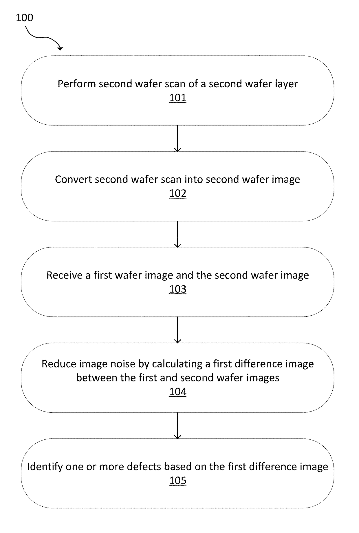
[0026]Although claimed subject matter will be described in terms of certain embodiments, other embodiments, including embodiments that do not provide all of the benefits and features set forth herein, are also within the scope of this disclosure. Various structural, logical, process step, and electronic changes may be made without departing from the scope of the disclosure. Accordingly, the scope of the disclosure is defined only by reference to the appended claims.

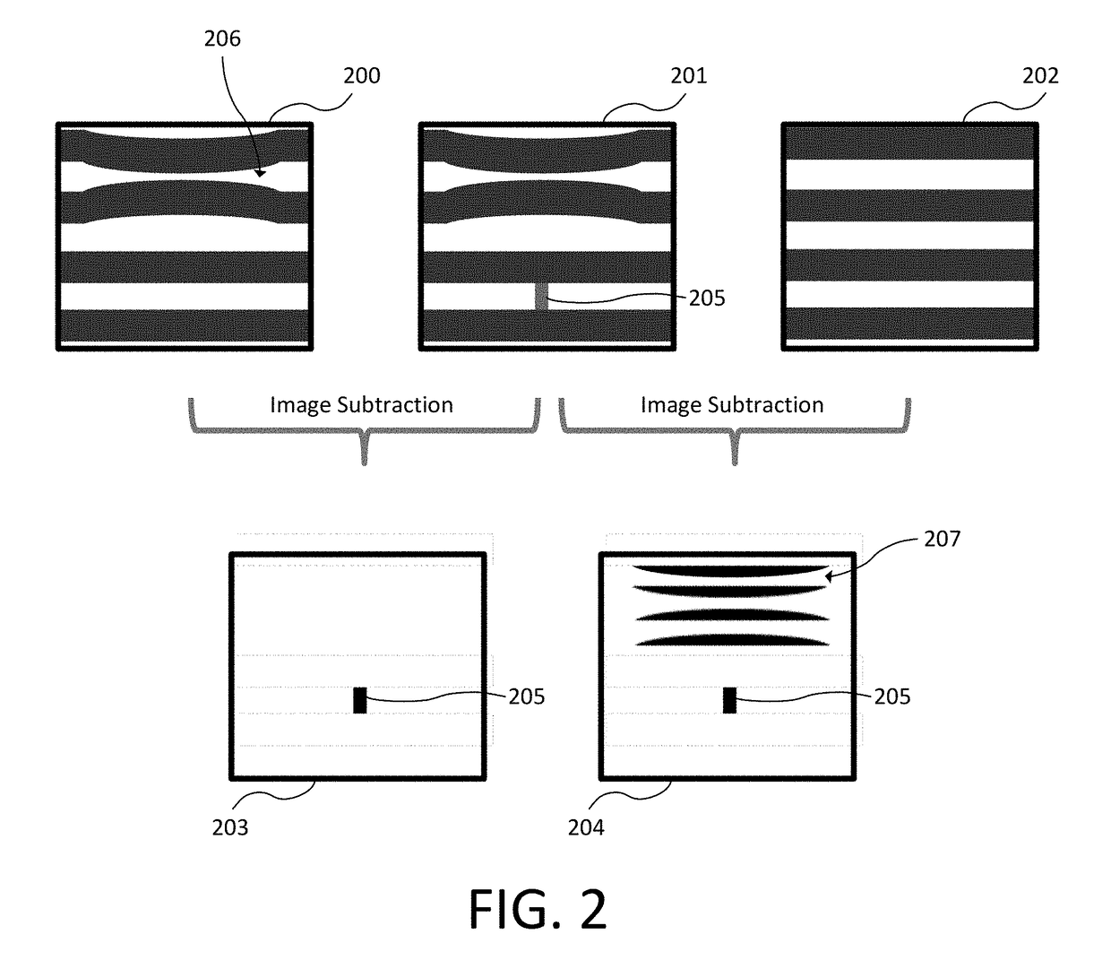
[0027]Embodiments of the methods and systems disclosed herein provide noise reduction in a difference image of an optical inspection tool by calculating a difference image across layers of a multi-layered wafer. Detection of defects that previously were buried in the noise floor (e.g., that have a signal to noise ratio that is generally too low for detection) is enabled. This can improve defect detection results for semiconductor manufacturers and increase throughput. In particular, pattern related defects such as missing...


PUM


Abstract

Noise reduction in a difference image of an optical inspection tool is provided by calculating a difference image across layers of a multi-layered wafer. A first wafer image of a first wafer layer and a second wafer image of a second wafer layer are used. The first wafer image and the second wafer image are at a same planar location on the multi-layered wafer, but of different layers and/or after different process steps. A first difference image is calculated between the first wafer image and the second wafer image to reduce wafer noise. Defects can be identified using the first difference image. A system with an image data acquisition subsystem can be used to perform this technique.

Description

CROSS-REFERENCE TO RELATED APPLICATIONS[0001]This application claims priority to U.S. Provisional Application No. 62 / 425,602, filed on Nov. 22, 2016, now pending, the disclosure of which is incorporated herein by reference.FIELD OF THE DISCLOSURE[0002]The present disclosure relates to reducing noise during defect detection.BACKGROUND OF THE DISCLOSURE[0003]Fabricating semiconductor devices, such as logic and memory devices, typically includes processing a substrate like a semiconductor wafer using a large number of semiconductor fabrication processes to form various features and multiple levels of the semiconductor devices. For example, lithography is a semiconductor fabrication process that involves transferring a pattern from a reticle to a resist arranged on a semiconductor wafer. Additional examples of semiconductor fabrication processes include, but are not limited to, chemical-mechanical polishing (CMP), etch, deposition, and ion implantation. Multiple semiconductor devices ma...

Claims


Application Information

Patent Timeline
Patent Type & Authority Applications(United States)
IPC IPC(8): G06T5/00G06T7/00G06T3/00G06K9/62G06T5/50
CPCG06T5/002G06T7/001G06T3/0068G06K9/6202G06T5/50G06T2207/30148G06T2207/20224G06V10/751H01L22/26H01L22/24H01L22/12
Inventor BRAUER, BJORN
Owner KLA TENCOR TECH CORP
Why Eureka
Try Eureka