Adhesive Composition And Use Thereof In Electronics

Inactive Publication Date: 2018-06-21
COMMISSARIAT A LENERGIE ATOMIQUE ET AUX ENERGIES ALTERNATIVES
View PDF0 Cites 1 Cited by
  • Summary
  • Abstract
  • Description
  • Claims
  • Application Information

AI Technical Summary

Benefits of technology

[0104]It will further be within the abilities of those skilled in the art to adjust the qua

Problems solved by technology

Even though existing adhesives may prove to be satisfactory, their operating temperature is not optimal.
Further, some of them appear in the form of pellets, making their use tedious in microelectronics.
Indeed,

Method used


Image

  • Adhesive Composition And Use Thereof In Electronics
  • Adhesive Composition And Use Thereof In Electronics
  • Adhesive Composition And Use Thereof In Electronics

Examples


Embodiment Construction

Preparation of Samples

[0113]A plurality of examples of adhesive compositions according to the invention have been prepared. To achieve this, the following components are mixed before the application of the adhesive composition onto a substrate:[0114]from 15 to 30 vol. % of a polysiloxane having a high rate of conversion into silica (Wacker's reference Silres®MK);[0115]from 60 to 85 vol. % of one or a plurality of inorganic fillers;[0116]a xylene-type solvent.

[0117]The volume contents are expressed with respect to the total volume of the adhesive composition except for the organic solvent.

[0118]The inorganic fillers used are thermally conductive and electrically insulating fillers with different grain sizes.

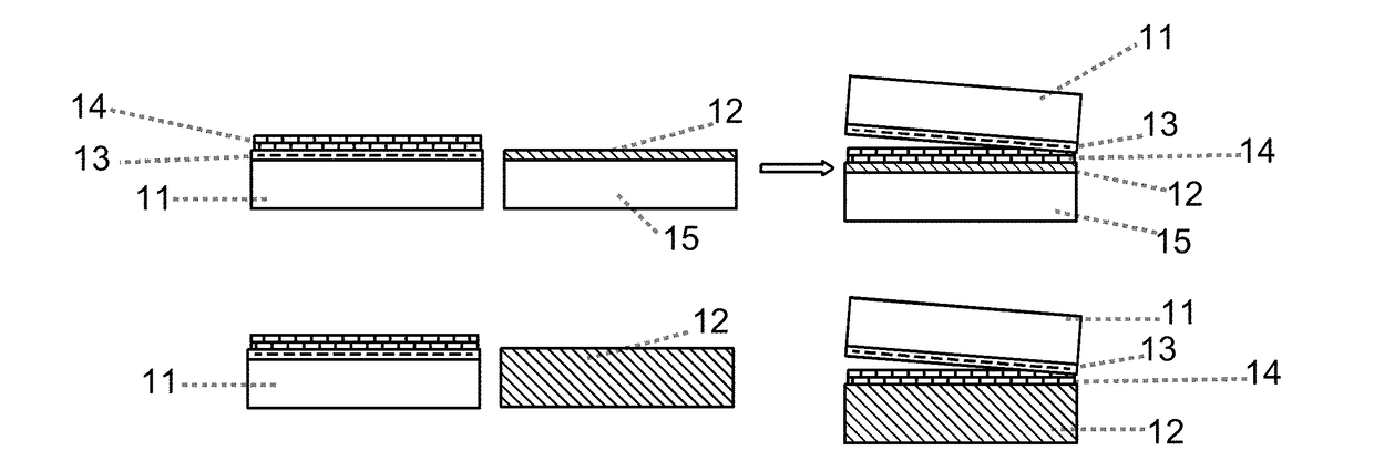
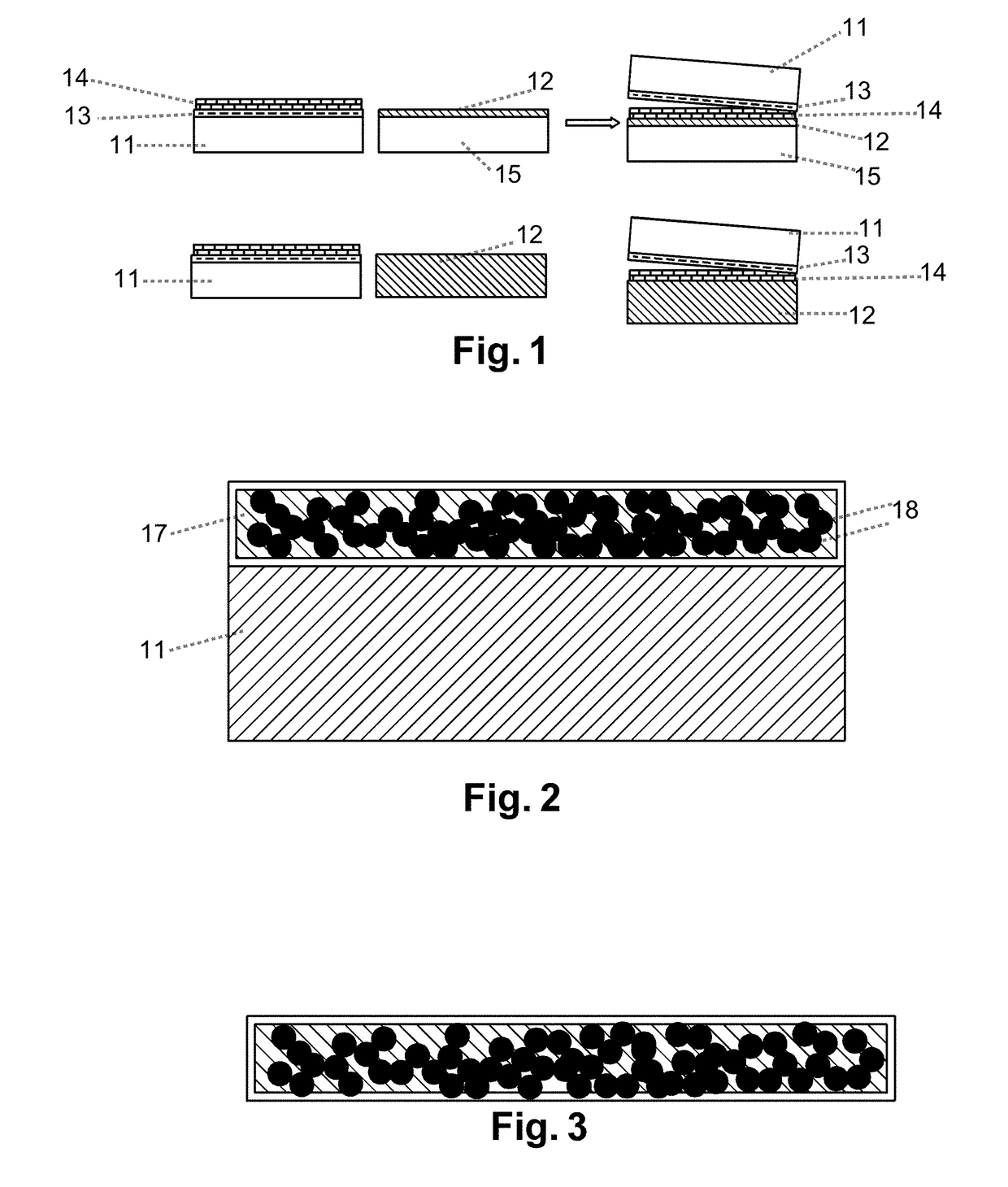
[0119]The adhesive composition is homogenized to distribute the inorganic fillers (18) within the preceramic polymer (17) (FIGS. 2 and 3). It is then deposited by spreading with a doctor blade on a silicon or silica substrate (11) (FIG. 2). It may also be used alone, that is, with...


PUM

PropertyMeasurementUnit
Lengthaaaaaaaaaa
Lengthaaaaaaaaaa
Nanoscale particle sizeaaaaaaaaaa

Abstract

An adhesive composition includes a polymer, inorganic fillers, and at least one organic solvent. The polymer is at least one preceramic polymer, advantageously based on silicon. The fillers include one or a plurality of thermally conductive and electrically insulating inorganic fillers.

Description

FIELD OF THE INVENTION[0001]The present invention relates to a thermally conductive and electronically insulating composition.[0002]The field of use of the present invention particularly relates to microelectronics, and more particularly to layer transfer methods.BACKGROUND[0003]Due the methods implemented, the manufacturing of microelectronic devices may require an adhesive which can be used over a wide temperature range. Further, it is preferable for this type of adhesive to have specific properties in terms of heat conduction and / or of electric insulation.[0004]More particularly, the manufacturing of a microelectronic device may comprise manufacturing one or a plurality of layers (14) on an initial substrate (11), and then transferring them onto a final substrate (12) possibly supported by a substrate holder (15), and this, by means of an adhesive (13) (FIG. 1).[0005]It is thus possible to form a complex architecture on a substrate capable of resisting the manufacturing condition...

Claims


Application Information

Patent Timeline
IPC IPC(8): C09J11/04C09J183/04
CPCC09J11/04C09J183/04C08K3/28C08K2003/282C08K2201/014C08K2201/011C08K9/00H01L2221/6835H01L2221/68363H01L2221/68368C08K3/013C08K2003/385C08K3/38C08K3/22C08K2003/382C08K2003/2227
Inventor ROUMANIE, MARYLINEFLASSAYER, CECILELAUCOURNET, RICHARD
Owner COMMISSARIAT A LENERGIE ATOMIQUE ET AUX ENERGIES ALTERNATIVES
Why Eureka
Try Eureka