Semiconductor Device, Display Panel, and Electronic Device

Active Publication Date: 2018-06-21
SEMICON ENERGY LAB CO LTD
View PDF7 Cites 15 Cited by
  • Summary
  • Abstract
  • Description
  • Claims
  • Application Information

AI Technical Summary

Benefits of technology

[0006]SRAM is capable of retaining data while power is on. Meanwhile, the amount of data retained in SRAM increases along with higher definition of a display device. To deal with the increase in data amount, transistors that constitute

Problems solved by technology

However, transistor miniaturization causes the increase in leakage current.
As a result, power consumption is increased in a source driver IC embedded with a frame memory using SRAM.
Moreover, when the power supply

Method used


Image

  • Semiconductor Device, Display Panel, and Electronic Device
  • Semiconductor Device, Display Panel, and Electronic Device
  • Semiconductor Device, Display Panel, and Electronic Device

Examples


embodiment 1

[0064]In this embodiment, an example of a semiconductor device functioning as a source driver IC will be described.

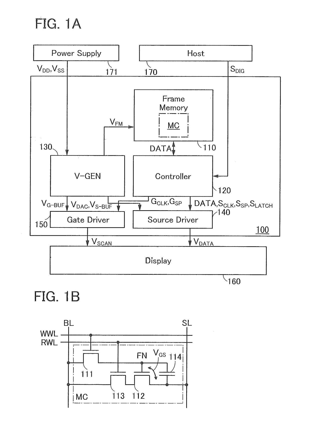
[0065]FIG. 1A illustrates an example of a block diagram that schematically shows a structure of a semiconductor device.

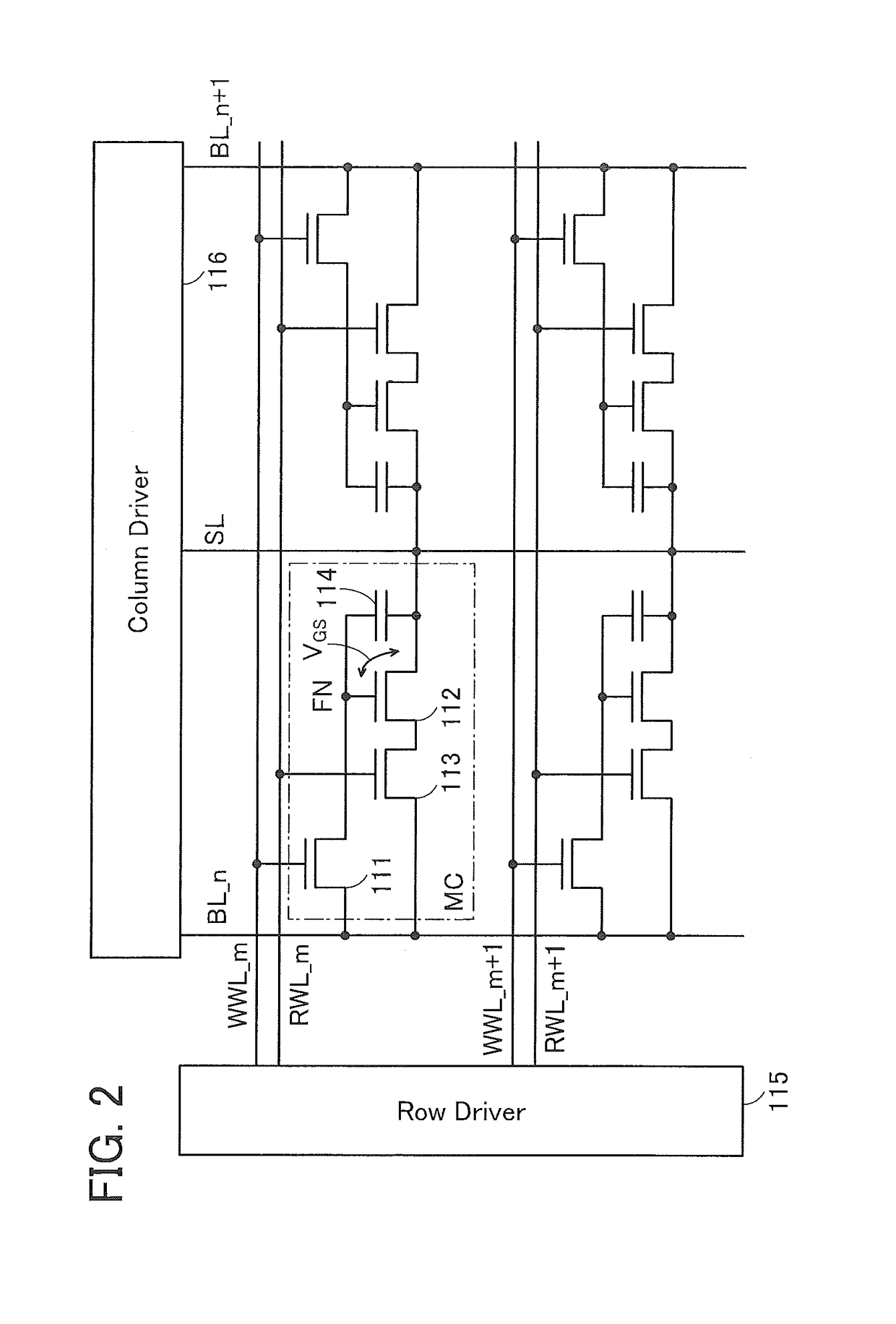
[0066]A semiconductor device 100 illustrated in FIG. 1A includes a frame memory 110 (shown as “Frame Memory”), a display controller 120 (shown as “Controller”), a voltage generator circuit 130 (shown as “V-GEN”), a source driver 140 (shown as “Source Driver”), and a gate driver 150 (shown as “Gate Driver”). The frame memory 110 includes a memory cell MC.

[0067]The frame memory 110 retains display data DATA for performing display in a display device 160 (shown as “Display”). The frame memory 110 writes and reads the display data DATA to / from the memory cell MC under the control of the display controller 120. A voltage VFM is supplied to the frame memory 110 from the voltage generator circuit 130.

[0068]A digital signal SDIG output from a host processor 170...

embodiment 2

[0127]This embodiment will describe the semiconductor device that is explained in Embodiment 1 and functions as a source driver IC, a display device driven by the semiconductor device, and their variation examples.

[0128]A block diagram of FIG. 16 illustrates the semiconductor device 100A, the host processor 170, the power supply 171, the gate driver 150, and the display device 160. In FIG. 16, scan lines XL[l] to XL[m], signal lines YL[l] to YL[n], and pixels 162 are shown in the display device 160. The semiconductor device 100A has a structure similar to that shown in FIG. 13 of Embodiment 1.

[0129]In the display device 160, the scan lines XL[l] to XL[m] and the signal lines YL[l] to YL[n] are provided to intersect at substantially right angles. The pixel 162 is provided at the intersection of the scan line and the signal line. For color display, the pixels 162 corresponding to the respective colors of red, green, and blue (RGB) are arranged in sequence. Note that the pixels of RGB ...

embodiment 3

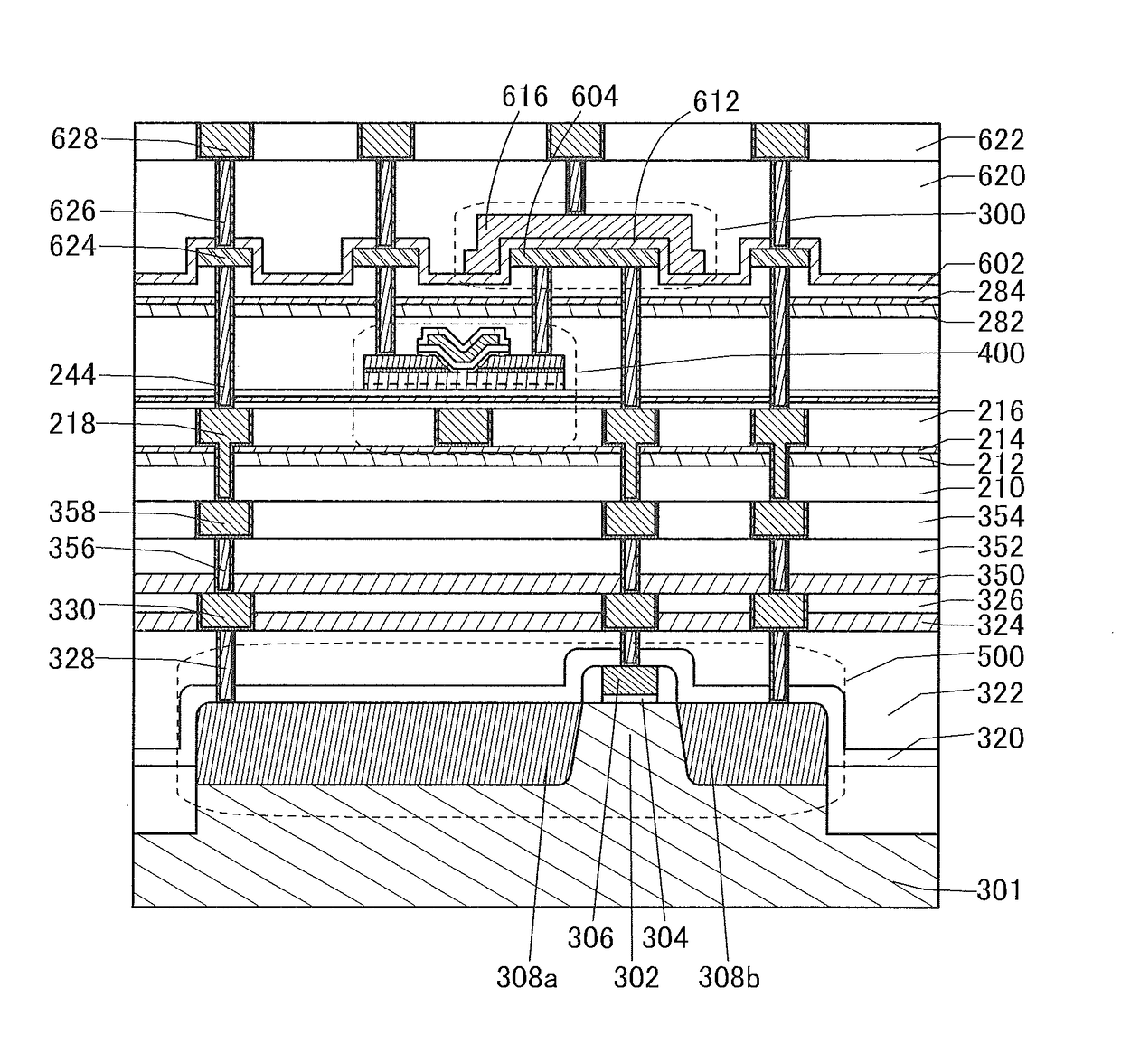
[0145]In this embodiment, an example of a cross-sectional structure of the semiconductor device in one embodiment of the present invention will be described with reference to FIG. 23 to FIG. 35.

[0146]The semiconductor device shown in any of the foregoing embodiments can be fabricated by stacking a layer including a transistor containing silicon (Si transistor), a layer including a transistor containing an oxide semiconductor (OS transistor), and a wiring layer.

[0147]FIG. 23 is a schematic diagram of a layer structure of a semiconductor device. A transistor layer 10, a wiring layer 20, a transistor layer 30, and a wiring layer 40 are provided to overlap each other in this order. The wiring layer 20 shown as an example includes a wiring layer 20A and a wiring layer 20B. The wiring layer 40 includes a wiring layer 40A and a wiring layer 40B. In the wiring layer 20 and / or the wiring layer 40, a capacitor can be formed such that an insulator is sandwiched between conductors.

[0148]The tra...


PUM


Abstract

Objects are to provide a semiconductor device with a novel structure, to provide a semiconductor device with high resistance to noise, to provide a semiconductor device with a small chip area, and to provide a semiconductor device with low power consumption. In a memory cell included in a frame memory, a transistor containing an oxide semiconductor and a transistor containing silicon are used in combination to retain charge, whereby data is retained. In this structure, turning off the transistor containing an oxide semiconductor can prevent data fluctuations even if power noise through a wiring is generated.

Description

BACKGROUND OF THE INVENTION1. Field of the Invention[0001]One embodiment of the present invention relates to a semiconductor device, a display panel, and an electronic device.[0002]Note that one embodiment of the present invention is not limited to the above technical field. The technical field of the invention disclosed in this specification and the like relates to an object, a method, or a manufacturing method. Furthermore, one embodiment of the present invention relates to a process, a machine, manufacture, or a composition of matter. Specific examples of the technical field of one embodiment of the present invention disclosed in this specification include a semiconductor device, a display device, a light-emitting device, a power storage device, a memory device, a method for driving any of them, and a method for manufacturing any of them.[0003]In this specification and the like, a semiconductor device refers to an element, a circuit, a device, or the like that can function by uti...

Claims


Application Information

Patent Timeline
IPC IPC(8): G11C11/419H01L27/12H01L27/11
CPCG11C11/419H01L27/1211H01L27/1108H01L29/24H01L27/1207H01L29/7869H01L29/7851H01L27/1116G11C7/02G11C11/405G11C11/4085H01L29/78648H01L29/78696G09G3/36G09G5/00G11C11/4072G11C11/4074
Inventor TAKAHASHI, KEIIKEDA, TAKAYUKITSUTSUI, NAOAKI
Owner SEMICON ENERGY LAB CO LTD
Why Eureka
Try Eureka