

Multilayer ceramic electronic device
a technology of electronic devices and ceramics, applied in the direction of fixed capacitors, stacked capacitors, fixed capacitor details, etc., can solve the problems of reducing reliability and reducing reliability, and achieve the effect of sufficient reliability
- Summary
- Abstract
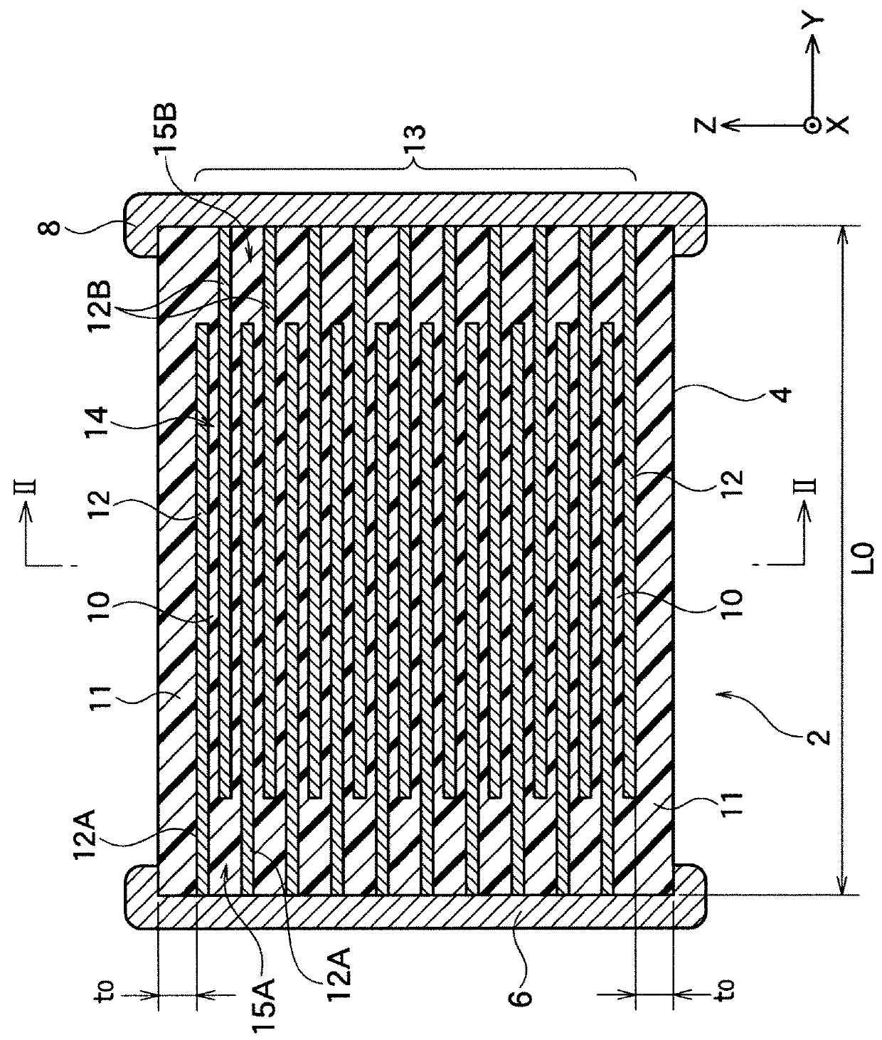
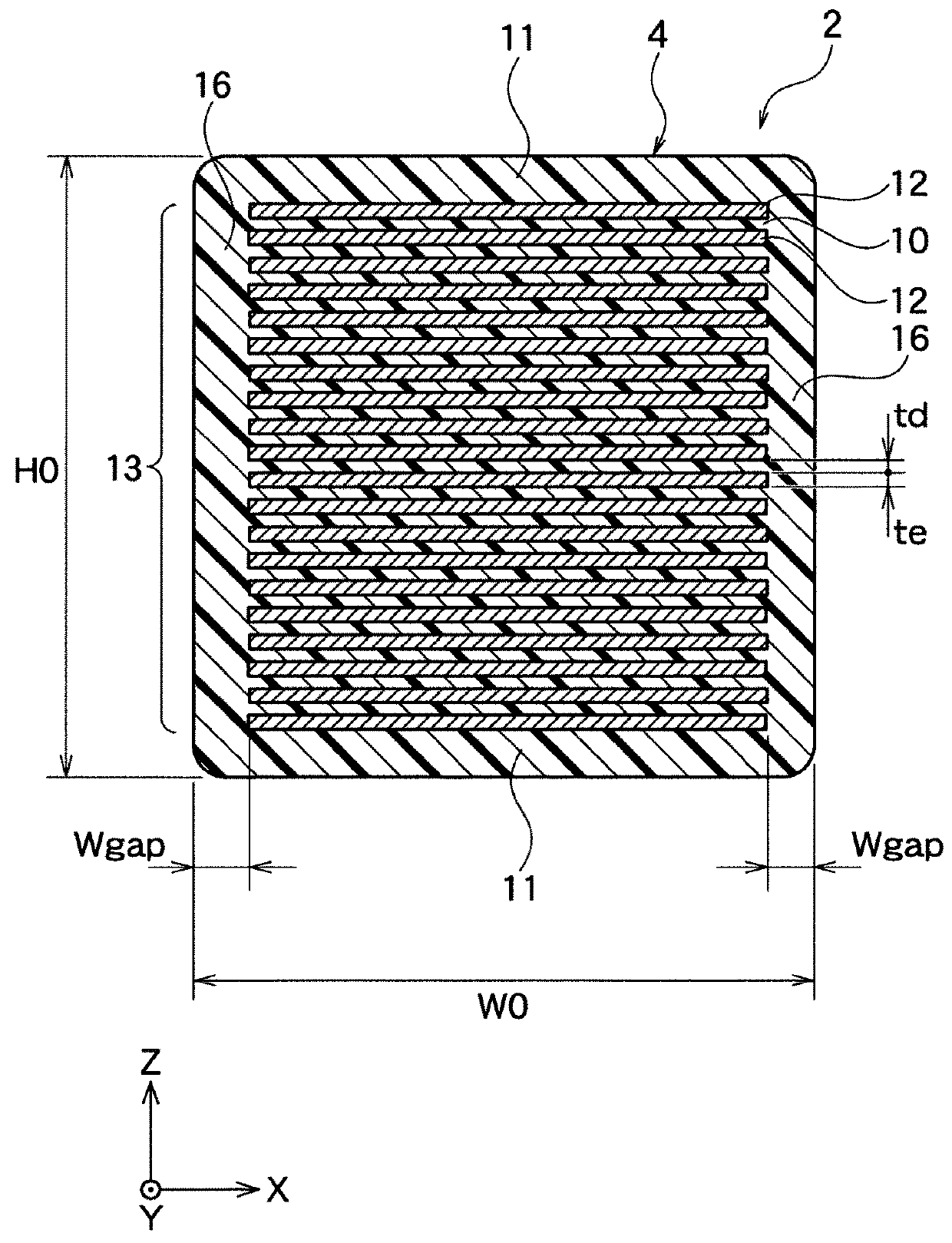
- Description
- Claims
- Application Information
AI Technical Summary
Benefits of technology
Problems solved by technology
Method used
Image

Examples
example 1
Preparation of Dielectric Layer Forming Paste
[0089]A ceramic powder having a main component of a BaTiO3 whose average particle size was 0.1 μm was prepared as a main raw material of dielectric layers. 10 wt % of a polyvinylbutyral (PVB) resin as an organic binder and 5 wt % of a dioctyl phthalate (DOP) as a plasticizer were respectively weighed and added to the main raw material. Thereafter, the main raw material was kneaded and turned into a slurry (dielectric layer forming paste).
Preparation of Internal Electrode Forming Paste
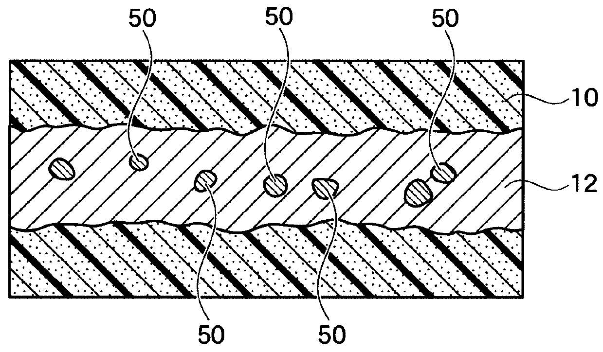
[0090]Ni particles whose average particle size is 0.1 μm were prepared. The Ni particles were added with 10 wt % (co-existent material amount) of a ceramic powder (ceramic particles whose average particle size was 0.03 μm) composed of BaTiO3. Moreover, 5 wt % of an ethyl cellulose resin and 35 wt % of a turbineol were weighed and added to the mixed powder. Thereafter, the mixed powder was kneaded in a ball mill, and an internal electrode forming paste was for...
example 2
[0103]Samples of Example 2 were manufactured in a similar manner to Example 1 except that the temperature rising rate in the firing step was changed from 25° C. / second to 50° C. / second, and were measured in a similar manner to Example 1. Table 1 shows the results.
example 3
[0104]Samples of Example 3 were manufactured in a similar manner to Example 1 except that the temperature rising rate in the firing step was changed from 25° C. / second to 100° C. / second, and were measured in a similar manner to Example 1. Table 1 shows the results.
PUM
| Property | Measurement | Unit |
|---|---|---|
| Fraction | aaaaa | aaaaa |
| Fraction | aaaaa | aaaaa |
| Thickness | aaaaa | aaaaa |
Abstract
Description
Claims
Application Information