Supercharge Your Innovation With Domain-Expert AI Agents!

Method of reconfiguring dq pads of memory device and dq pad reconfigurable memory device

Active Publication Date: 2018-07-05
SAMSUNG ELECTRONICS CO LTD
View PDF0 Cites 1 Cited by
  • Summary
  • Abstract
  • Description
  • Claims
  • Application Information

AI Technical Summary

Benefits of technology

This patent is about a method to change the mode of a DQ pad in a memory device while it is in use. This is possible by using metal layers, like M3 or M4, which can be used to connect the DQ pads to each other. By using this method, the memory device can have a smaller chip size and be more flexible in its use. Additionally, the method allows the DQ pad mode to be changed at any time during use, which improves usability and expands the range of applications for the memory device. The manufacturer can also produce a single memory device that can switch between multiple DQ pad modes, simplifying production and reducing costs. Purchasers can use the memory device without worrying about the DQ pad mode, increasing flexibility in its use.

Problems solved by technology

However, the users are not able to freely change the DQ pad mode according to the conventional memory device during use of the memory device.
In a limited number of metal layer structure, the introduction of a circuit to support changing the unit number of the DQ pads during use of the memory device causes a large overhead of the chip size of the memory device.
Therefore, the DQ pad mode cannot be changed during use of the memory device.

Method used


Image

  • Method of reconfiguring dq pads of memory device and dq pad reconfigurable memory device
  • Method of reconfiguring dq pads of memory device and dq pad reconfigurable memory device
  • Method of reconfiguring dq pads of memory device and dq pad reconfigurable memory device

Examples


case1

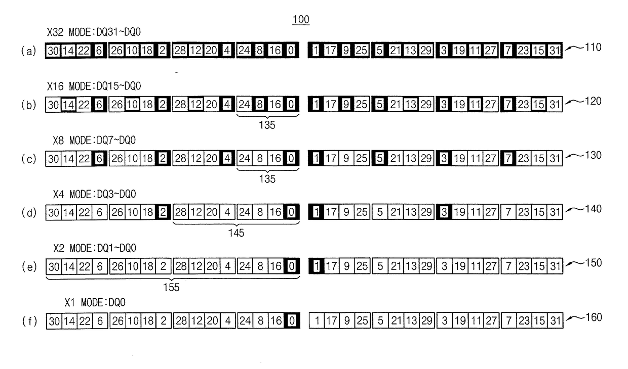
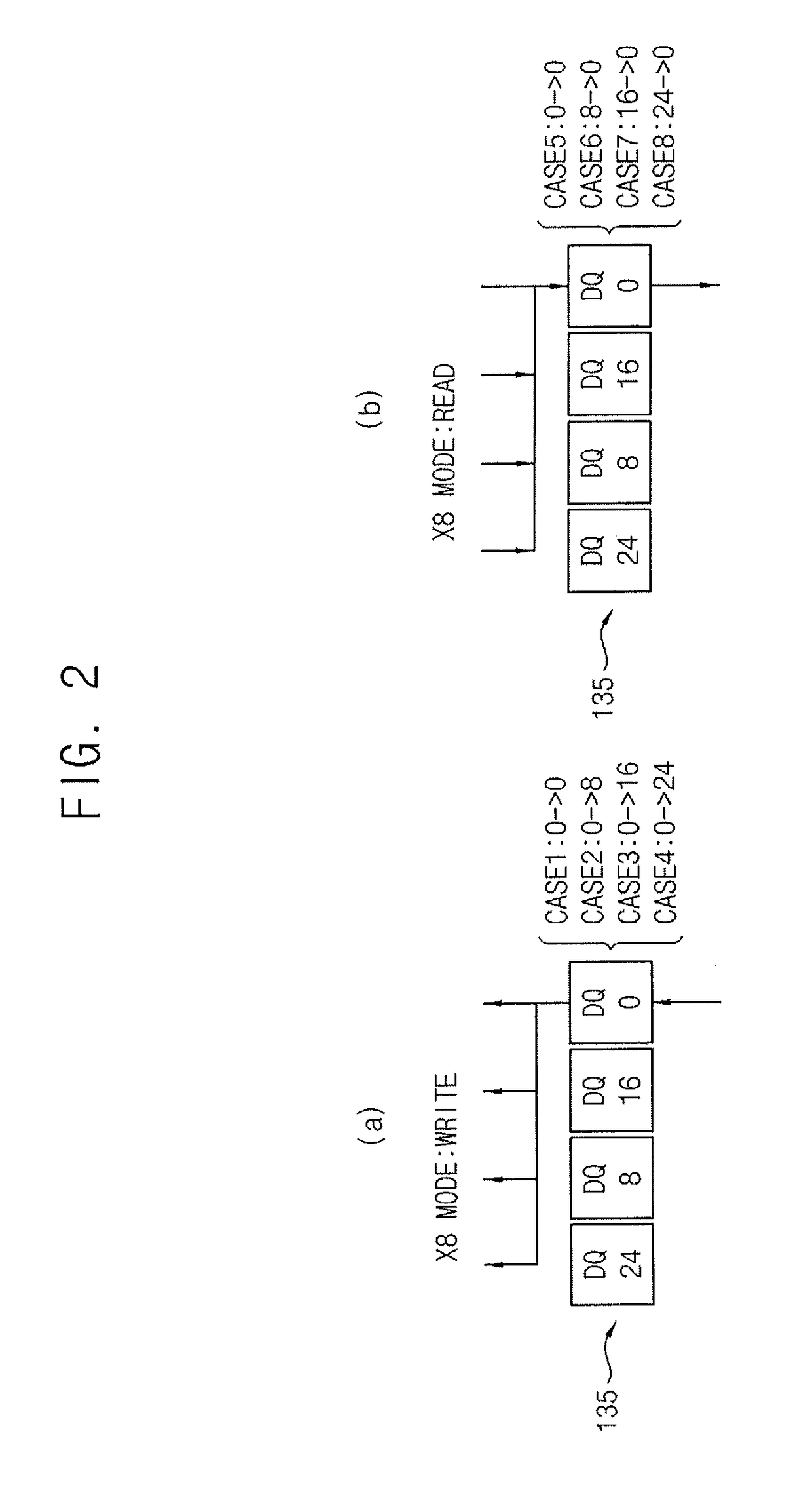
[0085 is a case in which the data in the memory cell array region corresponding to the DQ0 pad is output to the outside through the DQ0 pad. To do this, the two switching units 530 (S16) for the X16 mode and the switching units 540 (S8) for the X8 mode, which are associated with the first four-DQ pad group, need to be turned off. In addition, it is required that the switching unit 550 for the X4 mode and the switching units 560 and 570 for the X2 and X1 modes, which are provided in the read DQ organization reconfiguration circuit 500, also should be turned off. That is, for this the DQ organization reconfiguration control unit 260 can provide switching control signals of logic 0 to all of these switching units, namely, switching units 530, 540, 550, 560 and 570.

case2

[0086 is a case in which the data in a memory cell array region corresponding to the DQ16 pad is output to the outside through the DQ0 pad. For this case, the data in the memory cell array region corresponding to the DQ16 pad needs to be transferred from the read DQ selection circuit DQ′16 corresponding to the DQ16 pad to the read DQ selection circuit DQ′0 corresponding to the DQ0 pad. Therefore, only one switching unit, namely switching unit 530 (S16), connecting the two read DQ selection circuits DQ′0 and DQ′16 is controlled to be turned on, whereas all the remaining switching units, namely switching units 540, 550, 560 and 570, are controlled to be turned off.

case3

[0087 is a case in which the data in a memory cell array region corresponding to the DQ8 pad is output to the outside through the DQ0 pad. For this case, the data in the memory cell array region corresponding to the DQ8 pad needs to be transferred from the read DQ selection circuit DQ′8 corresponding to the DQ8 pad to the read DQ selection circuit DQ′0 corresponding to the DQ0 pad. Therefore, only one switching unit, namely switching unit 540 (S8), for connecting these two read DQ selection circuits DQ′0 and DQ′8 should be turned on. The remaining switching units, that is, the switching unit 530 (S16) for the X16 mode associated with the first four-DQ pad group, the switching unit 550 (S4) for the X4 mode provided in the read DQ organization reconfiguration circuit 500, and the switching units 560 and 570 (S2 and S1) for the X2 and X1 modes need to be controlled to be in the OFF state, respectively. The DQ organization reconfiguration control unit 260 provides signals for such switc...


PUM


Abstract

A method and a memory device therefor for reconfiguring a DQ pad organization of the memory device on-the-fly. A DQ organization reconfiguration control unit generates a control signal for reconfiguring the DQ pad organization into a desired mode based on a user command. A DQ organization reconfiguration unit is provided between P DQ pads and memory cell arrays and reconfigures organization P DQ pads on-the-fly in any one among Xi DQ pad modes, where i=1, 2, 4, 8, 16, 32, 64, and 128, based on the control signal. For the reconfiguration of the organization of the DQ pads, a plurality of bus lines for data transfer, being switchable by a control signal, are provided. The bus lines are implemented utilizing at least one of the M3 and M4 metal layers of the memory device.

Description

CROSS-REFERENCE TO RELATED APPLICATION[0001]This U.S. non-provisional application claims priority under 35 USC § 119 from Korean Patent Application No. 10-2017-0000446, filed on Jan. 2, 2017 in the Korean Intellectual Property Office (KIPO), the disclosure of which is hereby incorporated by reference in its entirety.BACKGROUND1. Technical Field[0002]Some embodiments of the present inventive concepts are directed to a memory device, and, more particularly to a method of freely converting a DQ pad organization of a memory device into a desired mode on-the-fly.2. Discussion of the Related Art[0003]In general, memory cells in a memory device are connected to the outside through DQ pads, that is, input / output pins (I / O pins). The DQ pads are used as an external interface. That is, DQ pads are used for data input and output to and from, respectively, the memory cells. During a write operation, a voltage (for example, high=1, low=0) is applied to a DQ pad, which is converted into an approp...

Claims


Application Information

Patent Timeline
IPC IPC(8): G06F13/40G06F13/12G06F3/00
CPCG06F13/4095G06F13/12G06F3/002G11C7/1039G11C7/1045G11C7/1051G11C7/1063
Inventor KIM, CHAN-KYUNG
Owner SAMSUNG ELECTRONICS CO LTD
Features
  • R&D
  • Intellectual Property
  • Life Sciences
  • Materials
  • Tech Scout
  • Unparalleled Data Quality
  • Higher Quality Content
  • 60% Fewer Hallucinations
Learn More