Method of producing an optical sensor at wafer-level and optical sensor
a technology of optical sensors and wafers, applied in the direction of photometry, instruments, electrical apparatus, etc., can solve the problems of optical sensors that are prone to error, source of error, and light that does not originate from ambient surroundings, so as to reduce limitations and risks, reduce cost, and add flexibility
- Summary
- Abstract
- Description
- Claims
- Application Information
AI Technical Summary
Benefits of technology
Problems solved by technology
Method used
Image

Examples
embodiment d
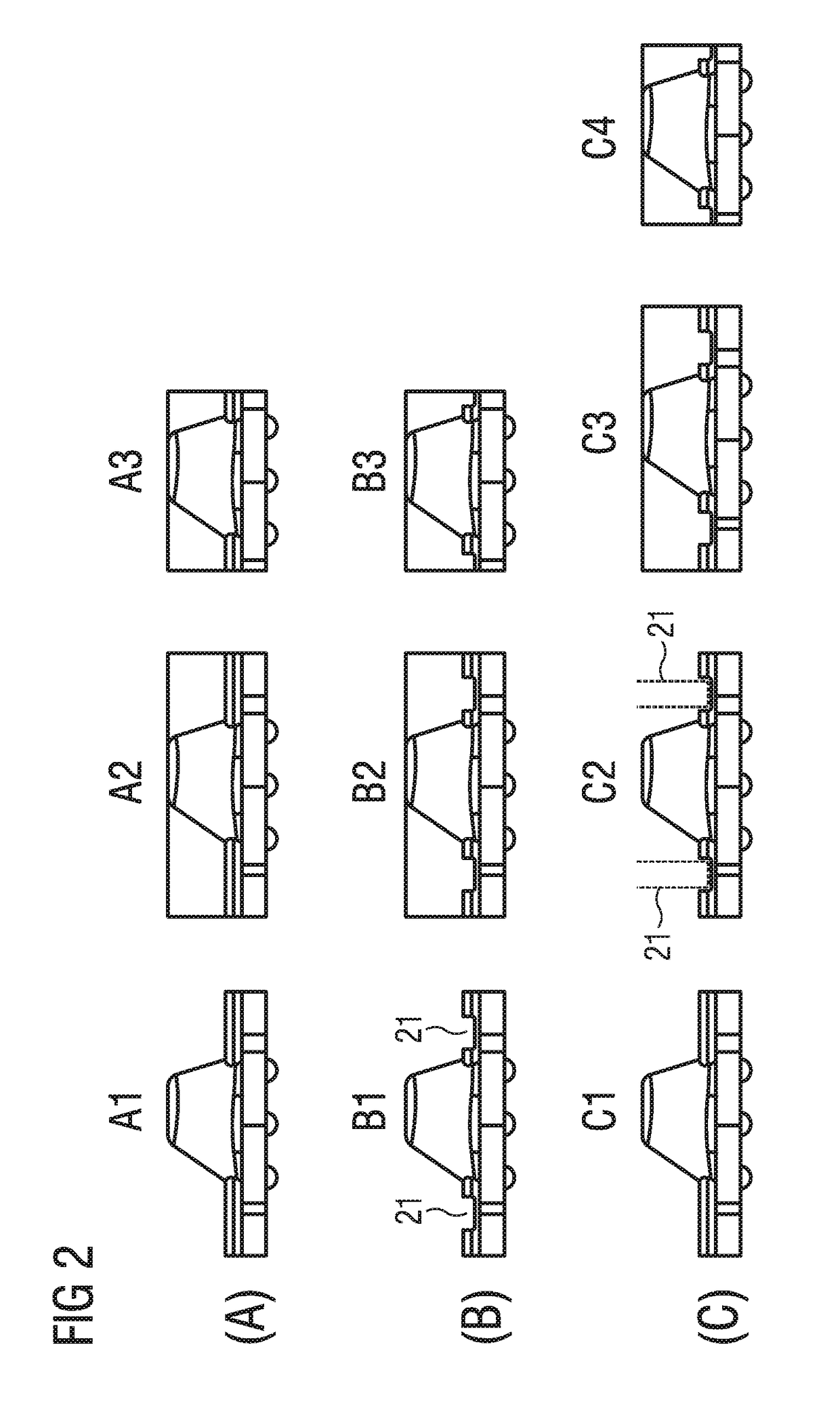
[0070 only differs from embodiment C in that the sawing step D2 completely cuts into the runners and further even partly penetrates into the substrate of the wafer. Thus, sawing may involve the runners 20 and, additionally, partial sawing of the saw street. Steps D1, D3, and D4 correspond to steps C1, C3, and C4, respectively.
[0071]Embodiment E involves runner removal by means of masking and etching. Steps E1, E5, and E6 correspond to steps C1, C3, and C4, respectively. However, in step E a mask layer 23 is applied over the transparent mold structure 2. The mask layer 23 at least partially covers the transparent mold structure 2. Most part of the runners 20, however, is not covered by the mask layer 23 and can be exposed to an etching substance.
[0072]In step E3 the runners 20 are removed by means of isotropic or anisotropic etching while the transparent mold structure 2 is protected from etchant by the masking layer 23 having a material which resists etching. Next, the mask layer 23...
PUM
 Abstract
Description
Claims
Application Information
 - R&D
- Intellectual Property
- Life Sciences
- Materials
- Tech Scout
- Unparalleled Data Quality
- Higher Quality Content
- 60% Fewer Hallucinations
Browse by: Latest US Patents, China's latest patents, Technical Efficacy Thesaurus, Application Domain, Technology Topic, Popular Technical Reports.
© 2025 PatSnap. All rights reserved.Legal|Privacy policy|Modern Slavery Act Transparency Statement|Sitemap|About US| Contact US: help@patsnap.com