Light irradiation type heat treatment apparatus and heat treatment method

a heat treatment apparatus and light irradiation technology, applied in the direction of dolls, toys, semiconductor/solid-state device testing/measurement, etc., can solve the problems of sudden thermal expansion on the front surface of the wafer to deform the semiconductor wafer in a warped form, and the temperature measurement error, so as to accurately measure the temperature of the upper surface of the substra

Active Publication Date: 2018-08-23
DAINIPPON SCREEN MTG CO LTD
View PDF0 Cites 11 Cited by
  • Summary
  • Abstract
  • Description
  • Claims
  • Application Information

AI Technical Summary

Benefits of technology

[0009]Even when the substrate is warped by irradiation with a flash of light, the substrate is hardly warped along the optical axis direction of the radiation thermometer, thus hardly changing the emissivity of the substrate, so that it is possible to accurately measure the temperature of the upper surface of the substrate.
[0021]Thus, an object of the present invention is to accurately measure the temperature of an upper surface of a substrate even when the substrate is warped by irradiation with a flash of light.

Problems solved by technology

In the annealing process, an annealing time period of several seconds or more causes deep diffusion of the implanted impurity by heat, resulting in a junction that is much deeper than is necessary to possibly cause an obstacle to favorable formation of a device.
It has been known, however, that in a flash lamp annealer, a front surface of a semiconductor wafer is instantaneously irradiated with a flash of light having extremely high energy, so that the temperature of the front surface of the semiconductor wafer rapidly increases in an instant, causing sudden thermal expansion on the front surface of the wafer to deform the semiconductor wafer in a warped form.
Such a warp of the semiconductor wafer during irradiation with a flash of light has caused a problem of generating an error in temperature measurement with a radiation thermometer.

Method used


Image

  • Light irradiation type heat treatment apparatus and heat treatment method
  • Light irradiation type heat treatment apparatus and heat treatment method
  • Light irradiation type heat treatment apparatus and heat treatment method

Examples


first preferred embodiment

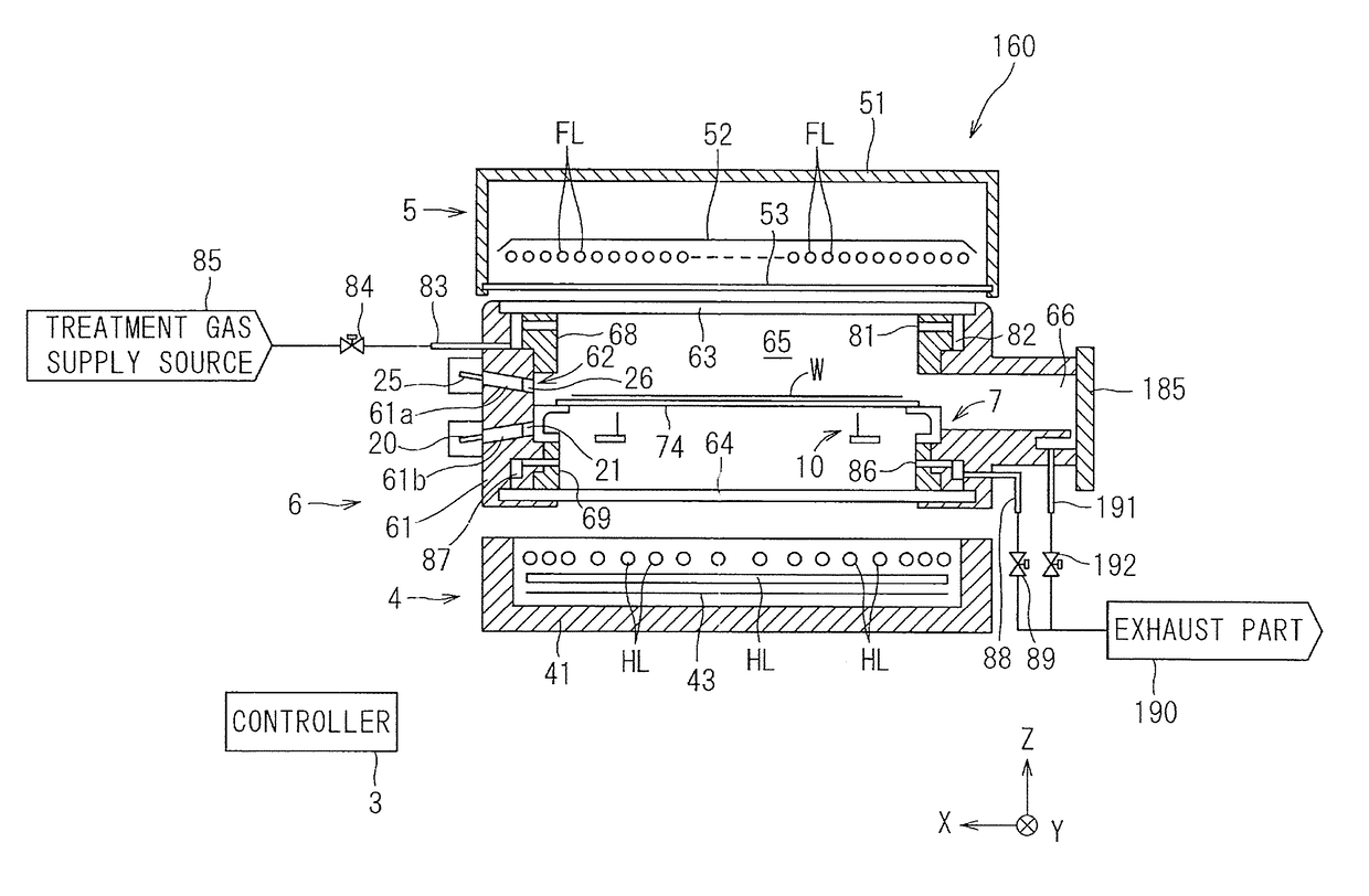
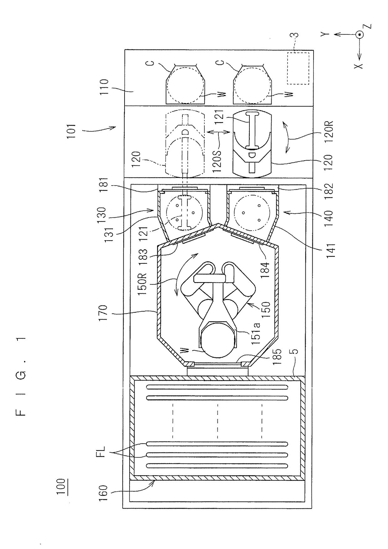
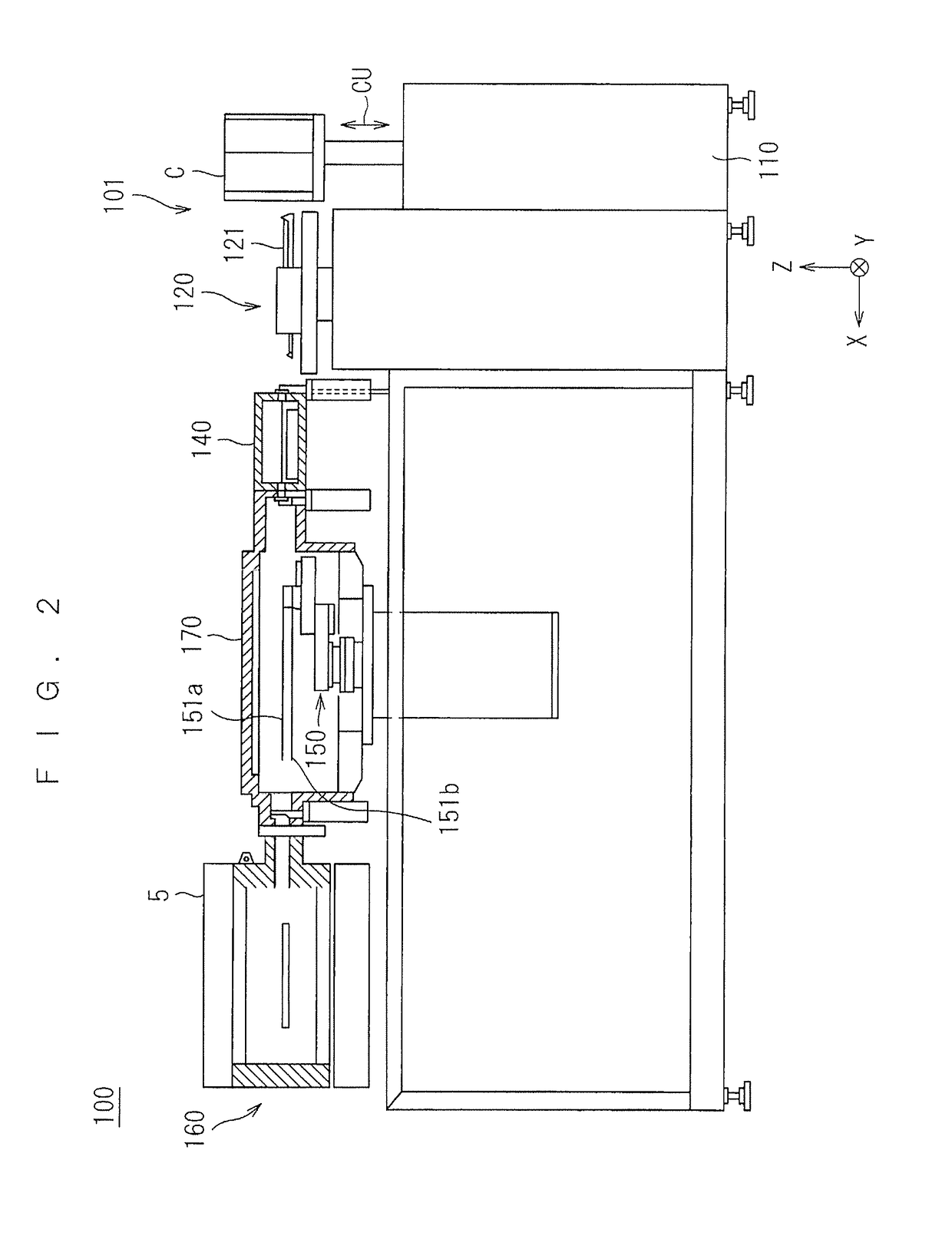
[0038]First, a heat treatment apparatus 100 according to the present invention will be briefly described in terms of an entire schematic configuration. FIG. 1 is a plan view showing the heat treatment apparatus 100 according to the present invention, and FIG. 2 is a front view of the heat treatment apparatus. The heat treatment apparatus 100 is a flash lamp annealer for irradiating a disk-shaped semiconductor wafer W serving as a substrate with flashes of light to heat the semiconductor wafer W. The size of the semiconductor wafer W to be treated is not particularly limited, and the semiconductor wafer W to be treated has a diameter of, for example, 300 mm or 450 mm. The semiconductor wafer W has an impurity injected therein before transported into the heat treatment apparatus 100, and the heat treatment apparatus 100 activates the injected impurity by a heat treatment. It should be noted that the dimensions and the number of components are shown in exaggeration or in a simplified f...

second preferred embodiment

[0118]Next, a second preferred embodiment according to the present invention will be described. The heat treatment apparatus 100 according to the second preferred embodiment is identical in the overall configuration and the configuration of the flash heating part 160 with that according to the first preferred embodiment. The procedure for the treatment of the semiconductor wafer W according to the second preferred embodiment is roughly similar to that according to the first preferred embodiment. The second preferred embodiment differs from the first preferred embodiment in adjustment of the direction of the semiconductor wafer W by the alignment part 130.

[0119]FIG. 13 is a view for illustrating adjustment of the direction of the semiconductor wafer W in the second preferred embodiment. In the first preferred embodiment, the direction of the semiconductor wafer W is adjusted on the basis of the fact that the semiconductor wafer W is, due to deviation in an in-plane temperature distri...

third preferred embodiment

[0122]Next, a third preferred embodiment according to the present invention will be described. The heat treatment apparatus 100 according to the third preferred embodiment is identical in the overall configuration and the configuration of the flash heating part 160 with that according to the first preferred embodiment. The procedure for the treatment of the semiconductor wafer W according to the third preferred embodiment is roughly similar to that according to the first preferred embodiment. The third preferred embodiment differs from the first preferred embodiment in that two upper radiation thermometers, a first upper radiation thermometer 25 and a second upper radiation thermometer 125 are provided outside the process chamber 6.

[0123]FIG. 14 is a view for illustrating adjustment of the direction of the semiconductor wafer W in the third preferred embodiment. As described in the second preferred embodiment, when the uniformity is high in an in-plane temperature distribution of th...


PUM


Abstract

A semiconductor wafer that has a plane orientation of (100) and is made of monocrystalline silicon is warped along an axis, i.e., a diameter along a <100> direction of the semiconductor wafer when irradiated with a flash of light. The semiconductor wafer is placed on a susceptor while the direction of the semiconductor wafer is adjusted so that the diameter along the <100> direction coincides with an optical axis of an upper radiation thermometer. This adjustment makes a diameter along a direction in which a warp of the semiconductor wafer is smallest during irradiation with a flash of light coincide with the optical axis of the upper radiation thermometer. As a result, the semiconductor wafer is hardly warped along the optical axis direction of the upper radiation thermometer even during irradiation with a flash of light, thus hardly changing the emissivity of the semiconductor wafer, so that it is possible to accurately measure the temperature of an upper surface of the semiconductor wafer.

Description

BACKGROUND OF THE INVENTIONField of the Invention[0001]The present invention relates to a heat treatment apparatus for irradiating with a flash of light a thin plate-shaped precision electronic substrate (hereinafter, simply referred to as a “substrate”) such as a disk-shaped semiconductor wafer to heat the substrate, and to a heat treatment method.Description of the Background Art[0002]In a process of manufacturing a semiconductor device, impurity introduction is an essential step of forming a pn junction in a semiconductor wafer. At present, an impurity is generally introduced by an ion implantation method and a subsequent annealing method. The ion implantation method is a technique of physically injecting an impurity by ionizing an impurity element such as boron (B), arsenic (As), and phosphorus (P) and making the impurity ion collide with a semiconductor wafer at a highly accelerated voltage. The injected impurity is activated by an annealing process. In the annealing process, a...

Claims


Application Information

Patent Timeline
Patent Type & Authority Applications(United States)
IPC IPC(8): H01L21/67H01L21/66H01L21/687
CPCH01L21/67115H01L21/67248H01L22/26H01L21/6875H01L21/68785H01L21/2253H01L21/2686H01L21/67288H01L21/681H01L21/68707H01L22/10A47F8/00A63H3/003A63H3/46
Inventor KITAZAWA, TAKAHIROFUSE, KAZUHIKO
Owner DAINIPPON SCREEN MTG CO LTD
Why Eureka
Try Eureka