Electronic component and method for manufacturing the same

a technology of electronic components and manufacturing methods, applied in the field of electronic components, can solve the problems of low product efficiency, achieve the effects of ensuring the conductivity of the outer surface of the element body, improving the speed of plating deposition, and facilitating the formation of metal films

Active Publication Date: 2018-08-30
MURATA MFG CO LTD
View PDF2 Cites 10 Cited by
  • Summary
  • Abstract
  • Description
  • Claims
  • Application Information

AI Technical Summary

Benefits of technology

[0004]In the above-described existing electronic component, the outer electrode is formed by the pastes containing the thermosetting resin and the Ag particles and the thermosetting resin is therefore interposed between the adjacent Ag particles. This causes a problem that a contact resistance of the outer electrode is increased to lower the efficiency of a product.
[0005]As a result of intensive studies, the inventors of the present application have focused on formation of an outer electrode by performing plating directly on a core in order to provide the outer electrode with a low resistance, and have reached the present disclosure. The present disclosure provides an electronic component in which an outer electrode with a low resistance can be easily formed, and a method for manufacturing the same.

Problems solved by technology

This causes a problem that a contact resistance of the outer electrode is increased to lower the efficiency of a product.

Method used


Image

  • Electronic component and method for manufacturing the same
  • Electronic component and method for manufacturing the same
  • Electronic component and method for manufacturing the same

Examples


embodiment

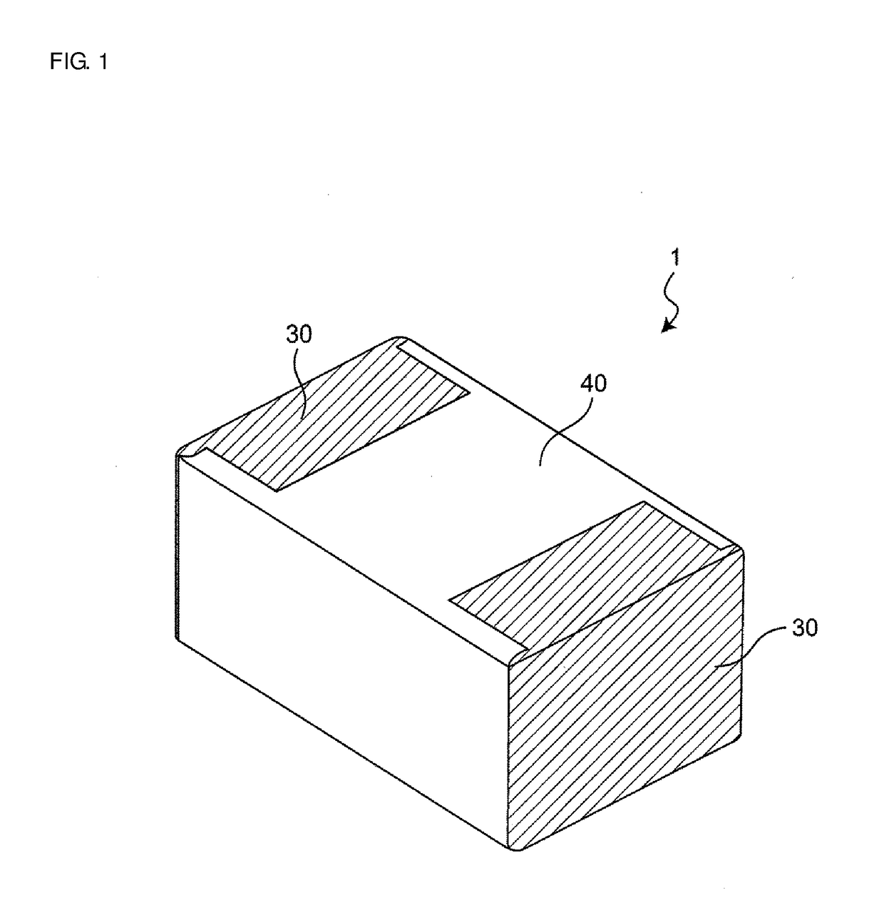
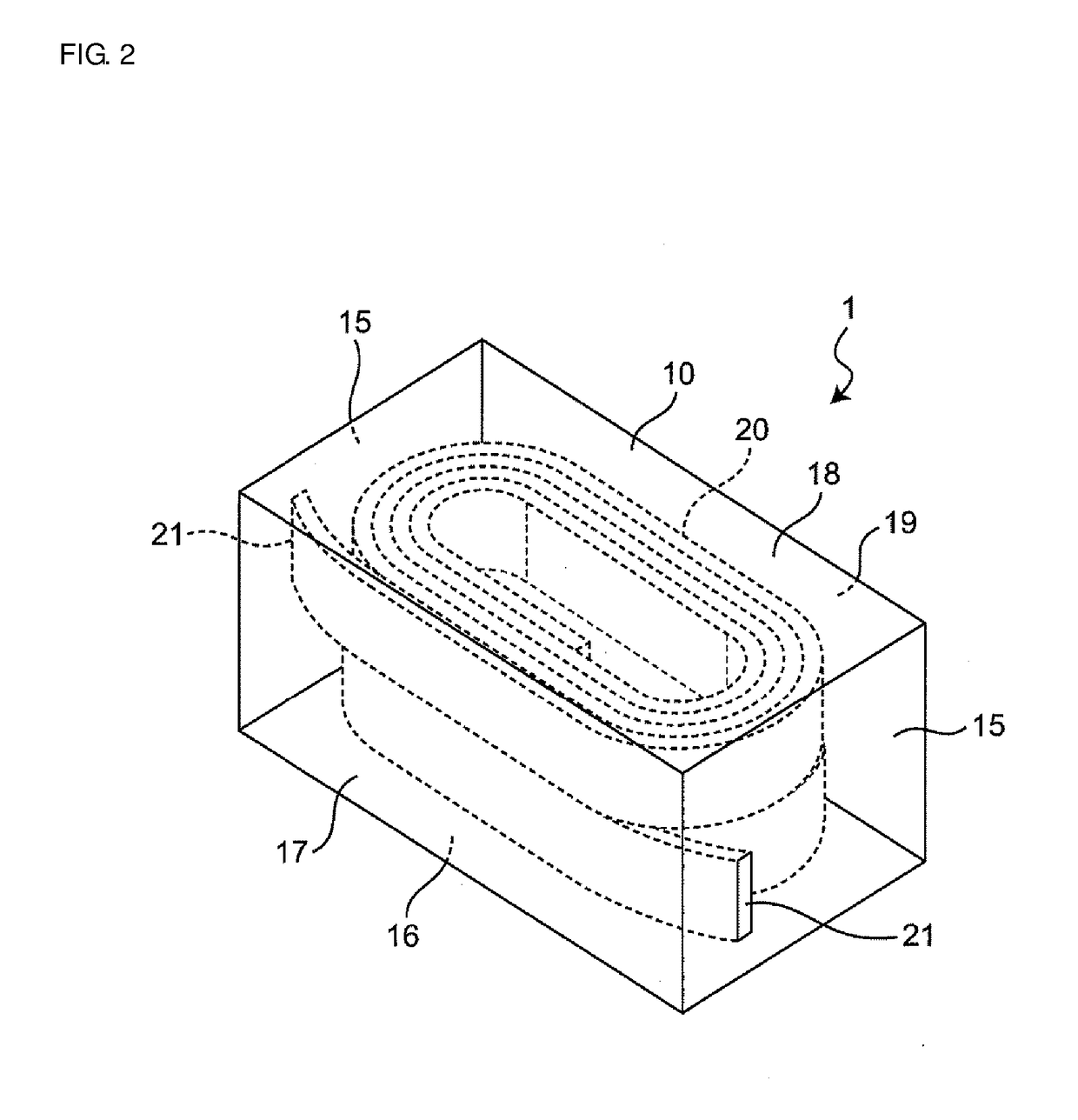
[0035]FIG. 1 is a perspective view illustrating an embodiment of an electronic component according to the present disclosure. FIG. 2 is a perspective view in a state in which the configuration of a part of the electronic component is omitted. FIG. 3 is a cross-sectional view of the electronic component. As illustrated in FIG. 1, FIG. 2, and FIG. 3, an electronic component 1 is a coil component. The electronic component 1 includes an element body 10, a coil conductor 20 that is provided in the element body 10, outer electrodes 30 that are provided on the outer surfaces of the element body 10 and are electrically connected to the coil conductor 20, and insulating films 40 that are provided on the outer surfaces of the element body 10. In FIG. 1, the outer electrodes 30 are illustrated in a hatched manner.

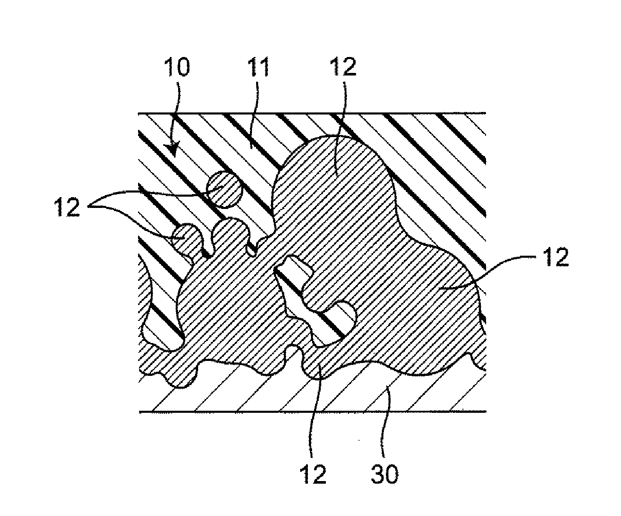
[0036]The element body 10 is made of a composite material of a resin material 11 and metal powder 12. Examples of the resin material 11 include organic materials such as polyimide res...

example

[0077]As illustrated in FIG. 9, the portions on which the outer electrodes are formed were irradiated with YVO4 laser having the wavelength of 1064 nm. Processing was performed with irradiation energy of 5 W / mm2 and 12 W / mm2. Then, reflection electron images of sites irradiated with the laser were shot with conditions of an acceleration voltage of 10 kV, an emission current of 40 μA, a WD of 10 mm, and an objective movable diaphragm of 4 using SU-1510 manufactured by Hitachi High-Technologies Corporation. Binarization decision of the metal powder and the other portions was performed on the shot images by image processing to calculate the area ratio (metal exposure ratio) of the metal powder. That is, the metal exposure ratio is defined as a ratio of the metal powder that is exposed in the exposure regions. Thereafter, the outer electrodes were formed by performing Cu plating by electrolytic barrel plating with conditions of a current value of 15A, a temperature of 55° C., and a plat...


PUM

PropertyMeasurementUnit
depthaaaaaaaaaa
particle size distributionaaaaaaaaaa
wavelengthaaaaaaaaaa

Abstract

An electronic component includes an element body made of a composite material of a resin material and metal powder. A plurality of particles of the metal powder are exposed from the resin material and make contact with one another on the outer surface of the element

Description

CROSS-REFERENCE TO RELATED APPLICATION[0001]This application claims benefit of priority to International Patent Application No. PCT / JP2017 / 001789, filed Jan. 19, 2017, and to Japanese Patent Application No. 2016-017042, filed Feb. 1, 2016, the entire contents of each are incorporated herein by reference.BACKGROUNDTechnical Field[0002]The present invention relates to an electronic component and a method for manufacturing the same.Background Art[0003]An existing electronic component has been disclosed in Japanese Unexamined Patent Application Publication No. 2013-211333. The electronic component includes a coil, a core made of a composite material of a resin material and metal powder and covering the coil, and an outer electrode provided on the surface of the core. The outer electrode is formed by applying pastes containing thermosetting resin and Ag particles to the core surface by dip coating.SUMMARY[0004]In the above-described existing electronic component, the outer electrode is f...

Claims


Application Information

Patent Timeline
Patent Type & Authority Applications(United States)
IPC IPC(8): H01F41/20H01F1/20H01F27/255H01F17/04H01F27/29H01F41/06B22F1/02H01F1/147B22F1/102
CPCH01F41/205H01F1/20H01F27/255H01F17/04H01F27/292H01F41/06B22F1/02H01F1/14733H01F2017/048H01F41/02B22F1/102B22F2998/10B22F1/10B22F2003/248B22F3/24C22C32/0094B22F2999/00C22C2202/02H01F17/0013H01F41/046H01F2017/0066H01F1/22B22F2202/01Y10T428/325
Inventor MUNEUCHI, KEITAISO, EIJIIDA, ISAOARAKI, KENICHISHIMIZU, NORIKOTOMOHIRO, TAKASHI
Owner MURATA MFG CO LTD
Why Eureka
Try Eureka